Mine's smaller than yours
Some things never change and while GlobalFoundries has been an independent company for a year now, it is still just as preoccupied with competing with Intel as it was when it was the manufacturing arm of AMD.
At MWC 2010 we spoke to VP of communications for GlobalFoundries - Jon Carvill - and he stressed that with a further investment of over $2.5 billion this year, GlobalFoundries will be first to market on smaller processes versus other foundries. He also said that, when GlobalFoundries starts making 28nm chips later this year, it will better even Intel, which isn't expected to move from 32nm to 22nm until late 2011.
"We've taped out 32nm products and will tape out 28nm Cortex A9 core in the second half of this year," said Carvill. "We're starting initial production at end2010/early 2011 and will be the most advanced at that point." Just to remind you, when we spoke to Intel's Pankaj Kedia at the show, he was keen to emphasise that Medfield will be the first low-power chip to be 32nm.
"28nm is the killer node for power efficiency for the mobile segment," said Carvill, stressing that the work with AMD - specifically the Llano ‘fusion' CPU at 32nm - has helped GlobalFoundries with the low-power work too.
We asked if the continued re-investment by parent company ATIC - and the consequent further dilution of AMD's ownership of GlobalFoundries, would create issues regarding the x86 license with Intel. "We now have our own independent arrangement to manufacture x86 products for AMD," said Carvill.
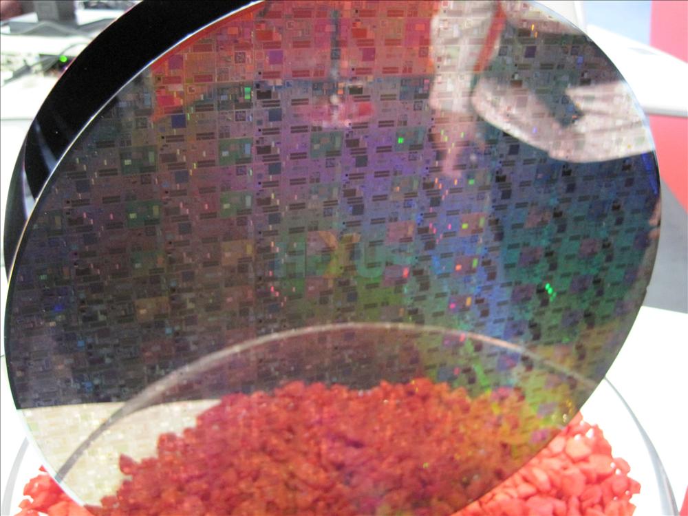
The development of the 28nm process at GlobalFoundries is being done in close collaboration with ARM, which designs a lot of the microarchitecture that will use it. While it's already complex enough to assess the competing claims of the various SoC-makers, it looks like manufacturing process will be as important a metric as any. Here's a photo of a 28nm wafer on the GlobalFoundries stand at MWC 2010.