The return of NVIDIA's Titanium
Between the GeForce GTX 560 Ti, GTX 570 and GTX 580, NVIDIA's 500-series product range has the £200+ gaming market pretty well sewn up.
But that's a small fraction of the overall landscape, and while the last-generation GTS 450 and GTX 460 continue to offer good value to the sub £150 crowd, NVIDIA's now looking to bring second-generation Fermi to the masses with the new GeForce GTX 550 Ti.

Taking aim at the mainstream
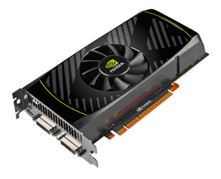
Launched in early March 2011, the £120 graphics card represents the next step down in the GeForce 500-series hierarchy from the £190 GTX 560 Ti, and as you might have guessed from the significant decrease in price, we're talking a fairly large step.
Built on the same tried-and-trusted 40nm process, the GTX 550 Ti is an evolution of the previous-generation's GTS 450 - both cards make use of a 238mm2; die packed with 1.17 billion transistors. And the similarities run deeper than that. Both the GTS 450 and GTX 550 Ti feature a single graphics processing cluster that's made up of four 48-core streaming multiprocessors (SMs).
That's an identical 192 CUDA cores apiece, but that's roughly where the similarities end. Cast your memory back and you might recall that the GTS 450's GF106 die utilised only two of a possible three memory-controller partitions, resulting in a 256KB L2 cache, two sets of eight ROPs and a 128-bit memory interface. Thanks to improved yields and transistor-level changes, the GTX 550 Ti's revised GF116 die makes full use of all three memory-controller partitions - that means a larger 384KB L2 cache, a total of 24 ROPs and a 50 per cent wider 192-bit memory interface capable of delivering almost twice the memory bandwidth.
And the improvements don't end there. With the added efficiency of the GF116 transistors, NVIDIA's able to boost frequencies across the board. Core clock rises to 900MHz (up from 783MHz on GTS 450), shader clock is boosted to 1,800MHz (up from 1,566MHz) and the card's 1GB frame buffer runs along merrily at an effective 4,104MHz. Notice anything peculiar? The 1GB frame buffer shouldn't be possible...
A memory mystery
Armed with half-a-dozen 32-bit memory controllers, NVIDIA was faced with something of a conundrum; does it equip the GTX 550 Ti with 768MB (6 x 128MB) or 1,536MB (6 x 256MB chips) of memory. The answer is neither. In an effort to match the GTS 450's 1GB frame buffer, the manufacturer has done something a little weird - it's used mixed-density memory chips; 4 x 128MB and 2 x 256MB.
It's an unusual approach to GPU memory, and NVIDIA must be confident that the mixed modules won't have a knock-on effect on latency. On paper, it has the required effect - GTX 550 Ti gets the desired 1,024MB of GDDR5 memory and sidesteps having to go into expensive-to-produce 1,536MB territory. Everyone's a winner, it seems.
Here's how all the numbers stack up:
| GTS 450 (1,024MB) | GTX 460 (768MB) | GTX 460 (1,024MB) | GTX 550 Ti (1,024MB) | GTX 560 Ti (1,024MB) | GTX 570 (1,280MB) | GTX 580 (1,536MB) | |
| Transistors | 1.17bn | 1.95bn | 1.95bn | 1.17bn | 1.95bn | 3.0bn | 3.0bn |
| Die size | 238mm² | 367mm² | 367mm² | 238mm² | 367mm² | 520mm² | 520mm² |
| Fermi revision | GF106 | GF104 | GF104 | GF116 | GF114 | GF110 | GF110 |
| General clock | 783MHz | 675MHz | 675MHz | 900MHz | 822MHz | 732MHz | 772MHz |
| Shader clock | 1,566MHz | 1,350MHz | 1,350MHz | 1,800MHz | 1,645MHz | 1,464MHz | 1,544MHz |
| Memory clock | 3,608MHz | 3,600MHz | 3,600MHz | 4,104MHz | 4,008MHz | 3,800MHz | 4,008MHz |
| Memory size | 1,024MB GDDR5 | 768MB GDDR5 | 1,024MB GDDR5 | 1,024MB GDDR5 | 1,024MB GDDR5 | 1,280MB GDDR5 | 1,536MB GDDR5 |
| Memory interface | 128-bit | 192-bit | 256-bit | 192-bit | 256-bit | 320-bit | 384-bit |
| Memory bandwidth | 57.7GB/s | 86.4GB/s | 115GB/s | 98.5GB/s | 128.3GB/s | 152GB/s | 192.4GB/s |
| SMs | 4 | 7 | 7 | 4 | 8 | 15 | 16 |
| Shaders | 192 | 336 | 336 | 192 | 384 | 480 | 512 |
| GFLOPS | 601 | 907 | 907 | 691 | 1,264 | 1,405 | 1,581 |
| L2 cache | 256KB | 512KB | 512KB | 384KB | 512KB | 640KB | 768KB |
| Texturing | 32ppc bilinear 32ppc FP16 | 56ppc bilinear 56ppc FP16 | 56ppc bilinear 56ppc FP16 | 32ppc bilinear 32ppc FP16 | 64ppc bilinear 64ppc FP16 | 60ppc bilinear 60ppc FP16 | 64ppc bilinear 64ppc FP16 |
| ROPs | 16 | 24 | 32 | 24 | 32 | 40 | 48 |
| ROP rate | 12.5 | 16.2 | 21.6 | 21.6 | 26.3 | 29.3 | 37.1 |
| GTexel/s bilinear | 25.1 | 37.8 | 37.8 | 28.8 | 52.7 | 35.1 | 49.4 |
| FP16 rate | 25.1 | 37.8 | 37.8 | 28.8 | 52.7 | 35.1 | 49.4 |
| Power connectors | 6-pin | 6-pin + 6-pin | 6-pin + 6-pin | 6-pin | 6-pin + 6-pin | 6-pin + 6-pin | 8-pin + 6-pin |
| Board power (TDP) | 106W | 160W | 160W | 116W | 170W | 219W | 244W |
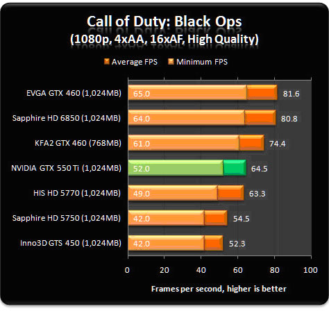
Going strictly by the above specifications, GTX 550 Ti won't offer enough oomph to best last year's GTX 460, but it should easily breeze past NVIDIA's own GeForce GTS 450 and the rival Radeon HD 5770 from AMD. Those performance credentials have been backed up by benchmarks from leading technology review sites:

Summary
NVIDIA's GeForce GTX 550 Ti graphics card is an evolutionary product that realises the full potential of last year's GTS 450. Inspired by the previous GF106 core, the new GF116 design introduces a third set of ROPs (resulting in a total of 24), a larger L2 cache, a wider 192-bit memory interface and increased frequencies across the board. The end result is a performance increase of up to 30 per cent.
Priced at around £120 at launch, the card offers strong mainstream performance for the budget gamer - but beware, both the NVIDIA GeForce GTX 460 and AMD Radeon HD 6850 offer greater performance for £10-£20 more.


