We are beginning to hear some interesting information leak out regarding the AMD Radeon R9 380X GPU. Two AMD employees have separately boasted of their involvement in this GPU's development as part of their LinkedIn profiles. It's good to keep your profile up-to-date but we think they might be a bit premature in discussing their parts in these 'achievements'. Actually Guru 3D has noted that one of the pages has already been edited to remove references to the upcoming product.
Ilana Shternshain, an ASIC physical design engineer and team leader at AMD, lists the following interesting morsels of information in her background summary page:
- Backend engineer and team leader at Intel and AMD, responsible for taping out state of the art products like Intel Pentium Processor with MMX technology and AMD R9 290X and 380X GPUs.
She goes on to list the following ASIC/layout design experience:
- AMD APU (incorporated into Sony PS4)
- AMD R9 290X GPUs
- AMD R9 380X GPUs (largest in "King of the hill" line of products)
Above we have more evidence of basically, not much more than, the name of AMD's next graphics cards series. However another eager LinkedIn member who works at AMD as a system architect manager, Linglan Zhang, shared some background detail on what is expected to be AMD's next generation of GPUs.
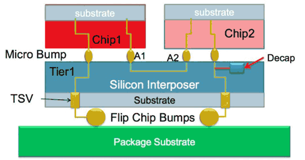
In some information pertaining to AMD's upcoming next gen GPU, Zhang wrote that he project managed the development of "the world's first 300W 2.5D discrete GPU SoC using stacked die High Bandwidth Memory (HBM) and silicon interposer."
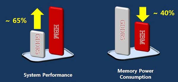
PCPer has looked into the background of HBM and found a diagram showing a 2.5D chip structure, as embedded below. With an HBM implementation the graphics memory would be located on the GPU chip substrate, said to be similar to how the Xbox One architecture works. This should provide benefits in performance and power consumption.
It is interesting to see how AMD is steering the next generation of its GPUs towards this 2.5D chip implementation. The last time we heard any rumours about the Radeon R9 300 series was back in November when ChipHell published a series of comparative benchmarks said to be taken with a Radeon R9 390X system codenamed 'Captain Jack'. These unconfirmed results showed a GPU offering a potent mix of great performance and very reasonable power consumption.