facebook rss twitter

Purported Nvidia GeForce GTX 2080 PCB photos leak

by Mark Tyson on 3 August 2018, 10:01

Quick Link: HEXUS.net/qadv5t

Add to My Vault: x

Please log in to view Printer Friendly Layout

Over at VideoCardz they have quite a few leaks regarding the upcoming next gen graphics cards from Nvidia. Last yesterday photos were shared on the site which are claimed to show a bare PCB of a GeForce GTX 2080 graphics card. The photo is nice and clear and there is a photo of either side of the PCB for enthusiasts to pore over.

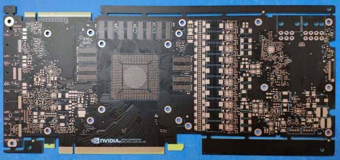
In the initial analysis by VideoCardz, who discovered the photos on Baidu, it is summed up that; the new card will sport either 8GB or 16GB of GDDR6 memory, there is a 10-phase VRM on this design, there are 6+8pin power connectors (the GTX 1080 only had a single 8-pin connector), and the model number and logo suggest this is not a custom board - actually it looks like a final reference design.

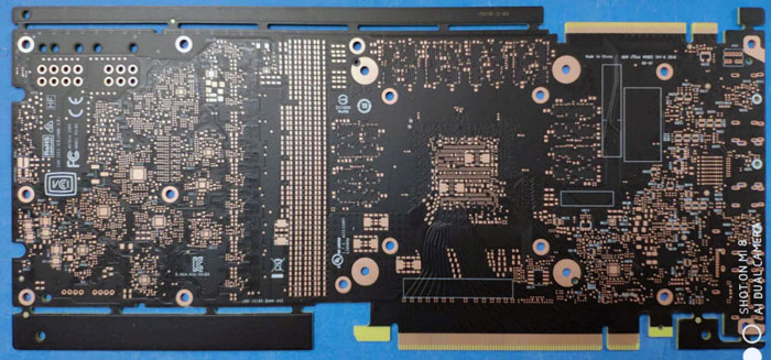
Elsewhere you can see that the GPU mounting area is rather modest in size. Along the top is a connector for what looks like NVLink. For a thorough analysis of the board and the questions it answers and raises the video below, from AHOC on YouTube is worth a gander.

That's not the end of the Nvidia leaks and spills yet, also on VideoCardz yesterday were some indications for the naming of the upcoming next gen GPUs and graphics cards series. One of Nvidia's Chinese graphics card partners, Manli, has registered a few codenames with the EEC, presumably to get ready for exporting new products over here.

Manli has registered the GA104-400 GPU. This will be the chip installed on the PCB pictured above. VideoCardz goes on to speculate that the GPU series might be dubbed Ampere, or something else beginning with A due to the 'A' in the codename. About an hour later, VideoCardz unearthed Manli's EEC registration of GeForce GTX 2080 and GeForce GTX 2070 products too.

The above upsets the apple cart somewhat, with regards to the names we were expecting for the next gen Nvidia GPUs and GeForce GTX graphics cards. However, we shall see for sure whether the Turing GPU series and GTX11 series 'brands' are really in the dustbin or not in the coming weeks.


HEXUS Forums :: 9 Comments

Login with Forum Account

Don't have an account? Register today!


The bottom PCB is for a GTX1080TI.

Looking at the size of the GPU pads,this looks smaller than than the GP102 in the GTX1080TI,so is under 471MM2.

I estimate around 400MM2 to 420MM2 in size,just comparing relative sizes(roughly).

Interestingly the GM204 in the GTX980 was around 398MM2.
CAT-THE-FIFTH
The bottom PCB is for a GTX1080TI.

Looking at the size of the GPU pads,this looks smaller than than the GP102 in the GTX1080TI,so is under 471MM2.

I estimate around 400MM2 to 420MM2 in size,just comparing relative sizes(roughly).

If the 1180 has the same number of shaders as a 1080ti but on a 12nm process, then that could be about right.
DanceswithUnix
If the 1180 has the same number of shaders as a 1080ti but on a 12nm process, then that could be about right.

TSMC 12NM isn't any denser than 16NM AFAIK but has improved leakage,so you build bigger GPUs or clock them higher(?),but I suspect moving to a 256 bit memory controller,means less space needed(which is why you are seeing a smaller chip?),and the shaders might be clocked higher.

However,its interesting that both the GTX1180 and GTX1080TI seem to use the same power connector arrangement,so it will be interesting to see how power consumption compares to the GTX1080 though!
CAT-THE-FIFTH
TSMC 12NM isn't any denser than 16NM AFAIK but has improved leakage,so you build bigger GPUs or clock them higher(?),but I suspect moving to a 256 bit memory controller,means less space needed(which is why you are seeing a smaller chip?),and the shaders might be clocked higher.

However,its interesting that both the GTX1180 and GTX1080TI seem to use the same power connector arrangement,so it will be interesting to see how power consumption compares to the GTX1080 though!

It was true that AMD didn't get a density improvement on Ryzen, but that was their choice. Wider tends to be better than higher clocked on GPUs, so it wouldn't surprise me if here they kept the clocks and went for more shaders.
DanceswithUnix
It was true that AMD didn't get a density improvement on Ryzen, but that was their choice. Wider tends to be better than higher clocked on GPUs, so it wouldn't surprise me if here they kept the clocks and went for more shaders.

Nvidia has gone the other way - every “new” chip has pushed clockspeeds higher and higher. AMD is the one who adds more and more shaders,until they hit the limit of what GCN can apparently handle.

Remember,the GP104 chip in the GTX1080 has 10% less transistors than the chip in the Titan Xm,and 20% less shaders. The GTX1080 had no problems beating a Titan Xm. It did it through more capable shader units and more clockspeed.

I mean it is quite possible Nvidia depreciates the shaders even more by making them use less transistors,and then packs more in,but since this is still a 16NM/12NM GPU,and its not like they have a whole ton of extra transistors to chuck at the problem.

Also,look at the power requirements,for a part with more efficient GDDR6,it does seem to need a 6 pin and 8 pin power connector. My GTX1080FE uses one 8 pin one.