Moore innovation
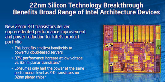
Intel has formally unveiled its 22nm chip manufacturing process, and with it a new type of transistor.
In shrinking the manufacturing process every two years, Intel has approached the limits of Moore's Law, that the number of transistors in a given chip area will double every two years. To be more precise, they can continue to shrink the process, but the benefits in terms of power and performance become less as electrical leakage increases.
The answer to this problem, it seems, is to move away from 2D - or planar - transistors, and towards 3D - or Tri-Gate - ones. There are all sorts of hard-core physics you can get into looking at how this works, and you can find out more in the video below, but the long and short of it is that 22nm chips will consume half the power at the same performance as 32nm chips, at twice the transistor density.
"Intel's scientists and engineers have once again reinvented the transistor, this time utilizing the third dimension," said Intel President and CEO Paul Otellini. "Amazing, world-shaping devices will be created from this capability as we advance Moore's Law into new realms."
"The performance gains and power savings of Intel's unique 3-D Tri-Gate transistors are like nothing we've seen before," said Mark Bohr, Intel senior fellow. "This milestone is going further than simply keeping up with Moore's Law. The low-voltage and low-power benefits far exceed what we typically see from one process generation to the next. It will give product designers the flexibility to make current devices smarter and wholly new ones possible. We believe this breakthrough will extend Intel's lead even further over the rest of the semiconductor industry."
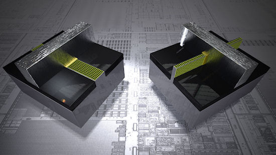
Planar (left) and Tri-Gate (right) transistor models
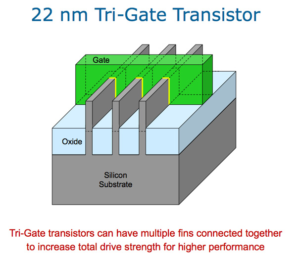
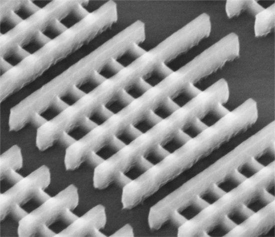
The transistor itself
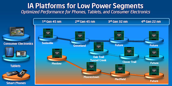
Regarding actual 22nm chips - codenamed Ivy Bridge - Intel kept it pretty vague, but implied we'd be looking at early next year for actual product on the market and that the first will be server chips. The Atom family will be addressed later in the year, and it was confirmed that this technology will also apply to 14nm. There were server, desktop and notebook demo units on show.
Intel said it expect this advantage to give its attempt to take on ARM a major boost. Intel insisted that the perception of ARM's architecture being intrinsically better for low-power was a misconception. Makes you wonder why Intel hasn't done better in that market.