Bob the Baker
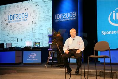
Putting some rather technical meat on the bones of Sean Maloney's IDF keynote, Intel VP Bob Baker took to the stage to give the audience some insight into what Intel does best; manufacturing.
After Otellini surprised the audience by whipping out a 22nm test wafer, almost two years to the day after showing off the now ‘almost current' 32nm, Baker was also allowed to hold the shiny round disc, and bask in its refracted glory, although the VP refused to show any pictures of the transistors that will make up its process geometry.
This could simply mean that Intel is purposefully dragging things out to stock up on talking points, which the firm can later rehash into further media announcements, or it could mean there has actually been further advancement in what is being touted as third-generation high K metal gate transistor technology.
Still, there's nothing like waving around a working 22nm, 2.9 billion transistor SRAM to prove the much repeated Mantra that Moore's Law is indeed still alive and kicking, but just how much more life the ‘law' has beyond 22nm is still an unanswered question.
To take a stab at answering that question, Baker invited Professor Jesus del Alamo from MIT to the stage to discuss the current research into III-V (3-5) materials, a purportedly promising avenue for keeping Moore's Law going. The explanation, although probably highly informative, sadly required a level of chemistry slightly beyond this hack, but suffice to say it made good use of the periodic table, especially columns 13 and 15, while Silicon sits all on its lonesome in column 14.
Moving on from advanced chemical engineering, Baker reiterated the importance of SoCs in Intel's future growth, even revealing that for every geometry (32nm, 22nm, etc.) there would be two processes: one for high performance CPUs and one for low power SoC chips. This is also, incidentally, something which has only really started with the 32nm generation, as the 45nm process for SoC was really just more of a tweak.
Baker also waxed lyrical about efficiency improvements to manufacturing capability, including a purported 25 per cent improvement in turnaround time for customer order placement to delivery, achieved over the past 21 months. Baker said this was crucial if Intel was to make headway with its SoC designs and turn customer requirements into working silicon in shorter times than it has been accustomed to in producing high-performance CPUs.
Of course, the cynical and jaded might say that Intel owes less of its success to occasional efficiency improvements and more to the fact it is financially and physically able to produce chips in absolutely massive quantities, making the finished product that much more economically viable.
Then again, if you've got it, flaunt it, and Intel is certainly not being shy with its new 22nm silicon beauties.