Samsung At The Heart Of SSD Innovation
There's every reason to consider solid-state drives (SSDs) as the primary storage medium for PCs and laptops. The benefit of SSDs over traditional spinning drives is immense. No moving parts enables smaller form factors to be created, while the intrinsic speed of SSDs far outstrip that of even the fastest mechanical spinners.
And there's more. The lack of moving parts is also a boon when copying or writing small files, as SSDs can be hundreds of times faster than traditional drives at these tasks. Want to speed up your computer? One of the cheapest ways to do this is to invest in an SSD.
However, not all SSDs are created equal. Composed of a controller and NAND flash memory, it is only the largest companies who can devote sufficient research and development resources to propel the SSD market forward through real innovation.
Those companies that manufacture their own NAND flash memory are at the vanguard of SSD development, and very few can offer the breadth of expertise exercised by Korean giant Samsung.
Samsung designs and manufacturers its own NAND memory, which makes up the bulk of the cost of an SSD. Samsung, too, develops the associated controller and software firmware that manages how the SSD interacts with the system. Such control over every facet of SSD development is one reason why Samsung is considered the premier manufacturer for both consumer and professional drives.
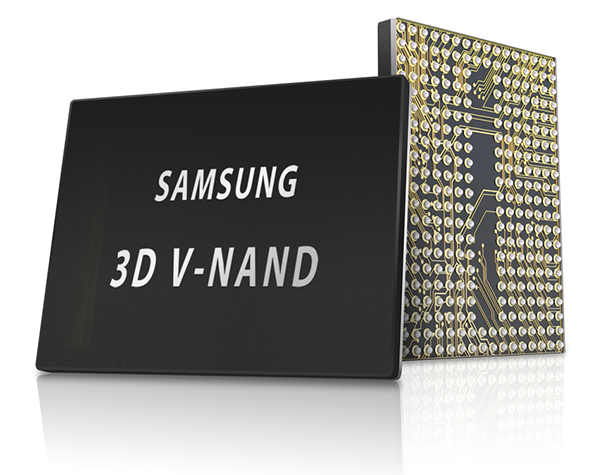
Pushing back the boundaries of NAND flash memory is a new technology developed exclusively by Samsung. Known as 3D V-NAND, the aim is to enable greater per-chip density and overall drive capacity by, in a nutshell, increasing the number of layers present on each NAND flash module. This is not easy task, mind you, and Samsung has spent years in perfecting the technique. 3D V-NAND is a big deal because it enables Samsung to increase capacity without having to reduce the size of the fabrication process, which can be extremely expensive to implement and has various pitfalls we'll discuss further on.
A New Way To Increase Capacity - 3D V-NAND
3D V-NAND is a cell layer-stacking technology where multiple layers are built up on a single NAND chip. Samsung implements up to 32 layers for the chips that go into the latest SSDs. Do be aware that the cells are stacked, not the chips themselves. More layers mean potentially more capacity, of course. V-NAND is great because it works on existing fabrication processes, such as the 10nm-plus class, helping mitigate problems of reduced endurance and poorer performance when NAND is scaled down further.
This is an important point. As memory cells are reduced in size by moving to smaller manufacturing processes one would expect lower operating voltages and more cells to fit into a given area, thereby increasing per-chip capacity, pivotal in the quest for 1TB-plus SSDs. While true to a reasonable extent, ever-smaller processes - where cells are located very, very close to one another - have a huge side-effect: interference. The proximity of cells causes interference that hampers the speed of overall chip. So while smaller fabrication processes are generally a good thing, they do also have unwanted problems. 3D V-NAND harnesses many of the benefits of small-fabrication chips but doesn't have their downsides.
Also, moving to a vertical 3D cell-stacking model means that compared to regular 'flat' planar NAND Samsung's 3D V-NAND requires less physical space for the same capacity - multiple cell layers are stacked on top of each other, remember - thus enabling mature fabrication processes to be used instead.
Reinventing The NAND Chip
There's more to 3D V-NAND than just stacking more layers on to a chip. Flash memory uses an electrically-isolated floating gate underneath the control gate of a transistor - CPU transistors only have a single gate - and its purpose is to increase the voltage threshold needed for the transistor to become conductive. When charge is put through the control gate to the floating gate, the memory is said to be programmed. Removing the charge erases the contents.
Samsung says that instead of using the traditional floating gate to add or remove charge coming from the control gate, which is extremely difficult to do when building for a 3D device, it's being supplanted by a charge trap, which is a non-conductive layer that effectively wraps around the transistor. This layer is crucial in minimising the interference between cells, has lower-leakage properties, and requires less voltage to function and therefore uses less energy. A by-product of lower voltage is less stress and increased endurance than would be possible by using a traditional floating gate.
Samsung has looked at the technology behind the chips that constitute the capacity of an SSD and engineered a method of increasing capacity, reducing power consumption and increasing the overall endurance... without having to go down the expensive, problem-ridden path of moving to a smaller manufacturing process. The move to 10nm, and smaller, will still happen in due course, but Samsung believes it makes more sense to use mature processes to minimise risk and keep NAND chips flowing from the factories. These enviable characteristics, in sum, enable Samsung to offer class-leading performance and power consumption on the latest array of consumer and datacentre SSDs.
Real-world Benefits
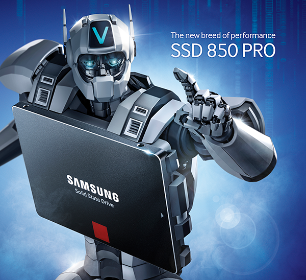
As an example of the various technologies rolled into a single drive, the Samsung 850 PRO's NAND uses the 32-layer version of the 3D V-NAND stacking technology. It is amongst the fastest consumer drives on the market and is available in up to 1TB capacities. Endurance, too, is excellent, thanks to the use of a charge-trap insulating layer instead of a traditional conductor.
Pertaining to SSDs, quality technology paves the way for increasing capacity and performance without sacrificing reliability and endurance. Samsung is leading innovation by implementing game-changing technologies such as 3D V-NAND into its latest drives.
Other manufacturers are sure to follow suit in time, underscoring Samsung's engineering prowess, but if you want the newest technologies baked into a high-performance SSD readily purchasable today, Samsung is, in late-2014, the only vendor to consider. Armed with 3D V-NAND, the Samsung 850 PRO is widely considered the premiere SSD for consumers and enthusiasts alike.
For full disclosure, this editorial was sponsored by Samsung.