


Examination and specs.
PC4000, DDR500, 250MHz FSB on the Pentium 4, cut it which ever way you want it, it all boils down to the same thing; speed. Generally speaking, and this is in the broadest possible terms that can be upset by many other factors, the greater the usable memory bandwidth, the better the performance in most memory-intensive benchmarks. The ability to pump more information into the CPU, with the assumption that it can actually use it, the more efficient it becomes for a given clock speed. That, really is why a 2.8GHz 800MHz FSB Pentium 4 is considered to be faster than the 533MHz variety. Hyper-Threading helps, but so does the increased front-side bus and memory bandwidth.That's why we see manufacturers eager to push faster speeds, especially with respect to the Pentium 4. Ask any enthusiast in the know and they'll inform you that running a CPU at 250MHz FSB is no big thing. Chipsets are able, and so are the lower speed CPUs. It's not uncommon to see a 2.4GHz 'C' hit 275MHz FSB (3.3GHz clock speed) at close to default voltage. The present problem is one of high memory MHz accompanied by high latencies. The latter undoes much of the good work of the former.
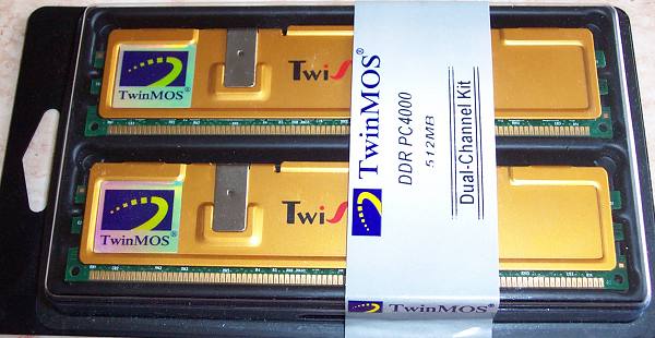
That brings us to TwinMOS' PC4000 Dual Channel Memory Kit. PC4000 memory is decidedly premium, still. TwinMOS usually gets away with bare RAM modules with the intention of attracting sales through aggressive pricing and no flowery presentation. These, however, arrive in a presentation box and with golden heatspreaders. Kits are available in 1GB (2 x 512MB) or 512MB (2 x 256MB).
The reasoning behind bundling them in matching kits is two-fold. Firstly, the major Pentium 4 chipset that focus on performance use dual-channel memory. That's 2 64-bit memory controllers combining to push out 6.4GB/s at 200MHz FSB. The P4's architecture, usually thought of as a quad-pumped FSB, allows it to use the quoted amount. NVIDIA's nForce2, too, uses a similar approach to inundate the Athlon XP with masses of bandwidth, which can't always be used. Secondly, the high-speed DC kits are almost exclusively for the Pentium 4. As mentioned, the CPUs, usually lower graded ones, and chipsets often have no trouble hitting 250MHz FSB. That's a potential 8GB/s of memory bandwidth and a raging 1000MHz system bus speed, as Intel likes to put it.
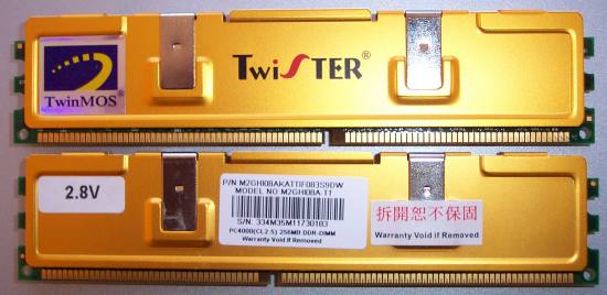
Shiny heatspreaders who's job it is to level out the heat buildup on the DRAM chips underneath. A by-product is a good-looking set of modules. The 'spreaders are aluminium. It's important to note that TwinMOS recommends a minimum 2.8v DDR for stable operation at DDR500 speeds. That's on the high side for present DRAM, and a number of motherboards' present BIOS limit. It's an indictment of DRAM supply today that voltages need to be increased to meet certain speeds. CPU manufacturing, for example, is always looking to go in the opposite direction.
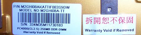
As for timings, a partial clue lies with the sticker. The set is rated to perform at DDR500 speeds with 2.5-4-4-8 latencies. That's one of the banes of ultra-high-speed operation, as we've mentioned previously. The desirable traits of low latency (thought of as response time) and high speeds (lots of bandwidth) are almost mutually exclusive. Mushkin has some excellent PC3500 memory that attempts to combine elements of both, but, in the main, you can have one or the other present at >DDR400 speeds.
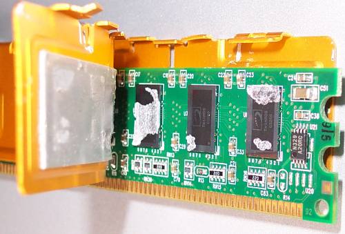
The modules don't use standard-looking chips. For the first time we see WLCSP packaging. Wafer-Level Chip Scale Packaging, to give it its full title and in the words of TwinMOS itself, refers to the packaging of the entire wafer instead of individual chips diced from the wafer -- a technique producing packaged chips 20% larger than the original. WLCSP involves packaging the entire wafer before the dicing process, producing packaged chips the same size as the original. WLCSP packaging also allows the chips to be placed on a PCB without the use of bonding wires. That's why it has such a clean-cut appearance. Improvements over TSOP RAM can include better electrical performance and smaller chip size. You can guesstimate just how small the individual chips are. They're arranged in 8 256Mbyte (32M x 8) chips, all along one side. The 512MB modules use the same chips but have both sides filled, giving 16 chips in total. Incidentally, TwinMOs also produces the same memory but in a standard TSOP package. The vendors need to differentiate between the two when describing the module.
Official specifications
JEDEC Standard
Bandwidth(max) 4.0GB/s
Date Rate 500MHz
Double Data Rate architecture
Bi-directional data strobe (DQS)
Different clock inputs (CK and /CK)
MRS cycle with address key programs
* CAS latency: CL2.5
* Burst length: 2, 4, 8
* Burst type: Sequential & Interleave
2 variations of refresh
*Auto refresh & Self refresh
Edge aligned data output, center aligned data input
2 banks to be operated simultaneously or independently
Serial Presence Detect with EEPROM
Package: TSOP, WLCSP
Nothing that we don't already know. 4GB/s of potential bandwidth per module. DDR500 operating speeds, albeit with 2.8v. No information is forwarded with respect to other timing parameters. Most PC4000 memory that we've laid our eyes upon has run with a CAS Latency of 3 clocks. 2.5 clocks, in that respect, may sound like an impressive improvement. The real-world implications are negligible. CAS latency isn't one of DDR's main performance determinants. Take down the tRCD to 2 clocks, however, and we'd be far more impressed.


