


Introduction
Athlon 64 with a touch of class
With AMD's new Athlon 64 processor over three months old now, we're beginning to see the birth of some excellent motherboards for the CPU to sit snugly into. The platform seems to have overcome that initial hurdle of consumer acceptance and now nearly everyone is building boards for the 754-pin powerhouse.
With NVIDIA dropping the ball ever so slightly with nForce3 Pro 150 and only expected to pick it back up with the Pro 250 variant early this year, it's been left to VIA to supply the chipset for the majority of the best boards hitting market just now. So while we've covered the FX-51 desktop Opteron variant (940 pins, needs registered memory, dual memory channel) recently, along with the more consumer oriented Model 3200+ (754 pins, single memory channel, unbuffered memory), it's worth having a mini refresher course on the CPU and VIA's chipset, for my benefit as well as yours.
Athlon 64
I'll just briefly run over the 754-pin version of the CPU here, since it's the version that'll power the focus of today's article. The FX-51 you can gawp at using the link above in the previous page section.At its core, Athlon 64 is the outgoing K7 with 2 more pipeline stages (so it does slightly less work per clock than K7 would with the same cache size), more L2 cache (doubled over Barton's 512KB, with the same layout), a new branch predictor to keep the pipeline busy, SSE2 SIMD implementation and the obvious introduction of the AMD64 ISA implementation. To top it off, the CPU carries the lowest latency DDR controller in the business.
With the memory controller on the CPU, there are obvious limitations when it comes to supporting new memory technologies, but overall it's an inspired move, one responsible for much of Athlon 64's performance in current applications, especially desktop and business apps. Games get their boost from the new 1MB of L2 cache memory.
So a 32-bit performance win all round really. 64-bit software support remains a distant future prospect, with Microsoft further dragging their heels with a desktop AMD64 version of Windows XP and hardware vendors reluctant to support it until that happens.
A key thing for Athlon 64 (non FX) is the support for unbuffered regular desktop memory, the stuff you are used to using in Pentium 4 and Socket A boards already. While the memory controller is single channel only, the performance suffers minimally. The other architecture enhancements more than make up for it and Model 3200+ can quite easily keep up with a 3.2GHz Pentium 4 on Canterwood in the majority of applications, even with a single memory channel.
I'll cover memory support later on when looking the test boards themselves.
VIA K8T800
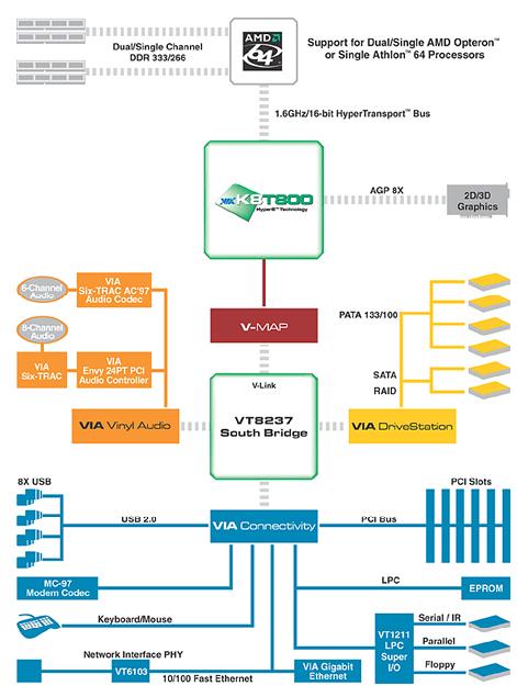
VIA's K8T800 core logic is a two chip design. The northbridge is connected by a full 16-bit wide HyperTransport bus link to the CPU. 800MHz in each direction gives rise to the 1.6GHz designation on the block diagram above. While the HT bus clock is driven from the derived CPU clock (in Model 3200+'s case, 200MHz x 10 for 2000MHz), the connected bridge determines its speed. With K8T800 that's 800MHz and 16-bit upstream and downsteam. NVIDIA's nForce3 Pro 150 is 600MHz maximum, 16-bit downstream, 8-bit upstream.
With the memory controller on the CPU, all the K8T800 northbridge really does now is connect to the CPU and provide a high performance AGP implementation. Of course it's AGP 3.0 compliant, providing an AGP8X slot and 2.1GB/sec of potential bandwidth for communicating with your graphics card. All high speed and seen on every recent chipset design in the last year and a bit.
A V-MAP design (V-MAP compatible chips share the same pin count and voltages, meaning drop in replacements on motherboard designs), K8T800 uses a 533MB/sec V-Link I/O path to the VT8237 southbridge. These days the southbridge (barring NVIDIA's all encompassing single chip design of course) is the business end of a core logic package. We take memory controller performance and AGP ports for granted, it's all about the features these days. VIA's VT8237 does all the hard work in K8T800 as a whole.
SATA first, the 8237 implements two native ports on the bridge that it can RAID up in 0, 1 or 0+1 fashions. A futher two ports may be provided by a two port PHY (Silicon Image's 3112 usually), taking the place of the secondary PATA channel on the bridge. So a bunch of different configurations for board makers to play with and lots of choice for us the consumers. Of course the PATA channels are ATA133 spec and the SATA is ATA150 natively, rather than NVIDIA's overclocked, bridged, attempt on nForce3 Pro 150.
As far as serial peripheral bus I/O goes, there's the ubiquitous support for eight USB2.0 ports, but no FireWire interface. However VIA provide a couple of complete FireWire ASIC solutions, the most popular being the VT6307, which gives two full powered FireWire400 ports. We hope most board makers will take advantage.
Audio next and it's here that VIA excels. There's a native audio interface on the 8237 that can feed a massive variety of sources, be it third-party CODECs from the likes of Realtek and Analogue Devices, or their own range of Vinyl Audio products. There's also support for their Envy24 series of ASICs, the top of the range being the Envy24PT, a full 7.1 output solution with 24-bit resolution, 96kHz recording and ASIO support. The Envy24 chips are full audio controllers in their own right, which need to feed CODECs on the far side of the connection from the 8237.
Lastly we have the Ethernet interface to which their VT6103 ASIC hooks up to for 100MBit/sec networking. Of course board makers can drop a networking controller onto the secondary PCI bus. The 8237 provides two, one for external devices like Ethernet controller and one for the PCI slots themselves. PCI2.1 in 32-bit, 33MHz form is all the 8237 supports, look for PCI-Express support in future bridges.
So there we have it, currently the highest performing Athlon 64 chipset, able to run single or dual Opteron, single Athlon FX or single Athlon 64, depending on the socket(s) provided by the motherboard maker. The feature set provided by the VT8237 along with all the helper ASICs and support for plenty of audio solutions, mean that it's a very flexible solution for board makers to build something around. No two boards should ever be exactly alike, given the range of choice.
That brings me nicely on to the reason for today's article. A few weeks ago I did a news post on HEXUS about a review of the K8V, mentioning how it was a board I've been interested in for a while. It appeared to take the best features of their P4G8X Deluxe, a Granite Bay, dual channel, Pentium 4 board I'd been a long distance fan of since its release, and apply them to Athlon 64 by way of K8T800.
ASUS' PR company in the UK noticed the news post and a day or so later a pair of K8V Deluxe boards arrived for me to take a look at. It appears the K8V is being sold in a number of guises at retail, three if I'm counting properly, and with two arriving, it's a double header review today. So, with K8T800 and Athlon 64 details locked away, let's take a look at the board first since it's common between all bundles, and then the bundles themselves afterwards, to see what all the fuss is about.


