|
 Asus A7N8X Deluxe 2.0
As we always do, lets take a look from left to right, top to bottom and see what we can see.
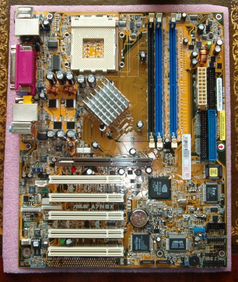
First up we hit the CPU socket area and straight away I hit a snag. It's a snag only idiotic reviewers that can't find their allen keys to remove Pentium 4 brackets from Swiftech heatsinks will hit, but my MCX462/478 with said brackets attached fouls on the row of 5 capacitors that flank the socket's south edge. While this isn't a problem for people that aren't using large mutated 80mm heatsinks, it does mean the area around the socket isn't as vast as you'll find on other boards. A recent Leadtek passes this extreme test. You do of course get the 4 mounting holes you'd need for less overweight lumps of copper and aluminium.
Carrying on from the socket area we hit the three colour coded DIMM slots for your DDR memory. Of course, TwinBank operation is preferred on nForce2 and to this end, ASUS have helpfully colour coded the slots. The two slots closest to each other, blue and black, share a memory controller on the SPP and therefore you'll want to populate one of those and the lonely blue slot for successful TwinBank dual channel operation.
Past the DDR slots you'll reach the ATX power connector. It's been a while since I've come across far right board placement for this connector and I have to say I'm not a fan. If you don't possess something like an Enermax with its snake-like ATX power cable, routing yours to avoid dragging it across the CPU area could be a problem. Snuggling up tight to the ATX connector on the board is the floppy connector and the pair of parallel ATA connectors for your regular common or garden hard drives and ATAPI optical devices. The days of 4+ SerialATA ports and a single 'legacy' parallel connector for optical devices can't be that far off. We can but hope.
Encroaching more on the socket area than the AGP slot unlike their Springdale solution, the passively cooled northbridge is the next board feature worth more than a passing glance. Passive equals no noise equals thumbs up. Quiet good, noisy bad. Two fan connectors and a bizzare spiral copper component that I can't name sit just below the northbridge and its cooler and just above the AGP slot.
Talking about the AGP slot and the area around it which has become something of a hot topic with the recent advent of the space stealing Zalman passive graphics card coolers, it looks like the slot on the A7N8X 2.0 will pass that particular Zalman test without a hiccup, especially on the north side.
Just below the AGP slot (AGP8X and 'Pro' no less) sits a rotated MPC-T southbridge. Such a tiny package and such hidden goodies. Far right along the leading edge of the board across from the MCP-T sits the IT8708F-A legacy I/O controller. It runs the rather unsexy PS/2, serial and parallel ports and other such unused nonsense. ABIT had the right idea with the original MAX boards, get rid of this cack.
5 PCI slots next, all in a row. And with that revelation we are just about done. However the bottom right corner of the board screams out that we should look at it and to be fair, it deserves some attention. We have everything from the Silicon Image SerialATA controller, the ports for said controller, our USB2.0 header and various headers for things like your case connectors and infra red port. There's PCB space for an ACR connector but who cares, the port isn't there thankfully.
Just before we finish our look at the layout, over in the bottom left beside the modem audio header are the tiny PHY's for the Ethernet MAC's, with the one for the audio near PCI2.
Unwrapped, hooked up and manual skimmed through, what happens when you flick the power switch?
|


