Intel CEO Pat Gelsinger hosted an hour-long global 'Intel Accelerated' webcast yesterday evening. There are numerous highlights from the event to discuss, and in our headline you can see that Intel announced plans for a new node naming scheme, sharing a roadmap to 2025+. Other interesting titbits were on the topics of; two new process technologies (RibbonFET and PowerVia), the claimed leadership in 3D packaging (Foveros Omni and Foveros Direct), and news of progress for Intel Foundry Services (IFS) with Qualcomm announced as the first major customer.
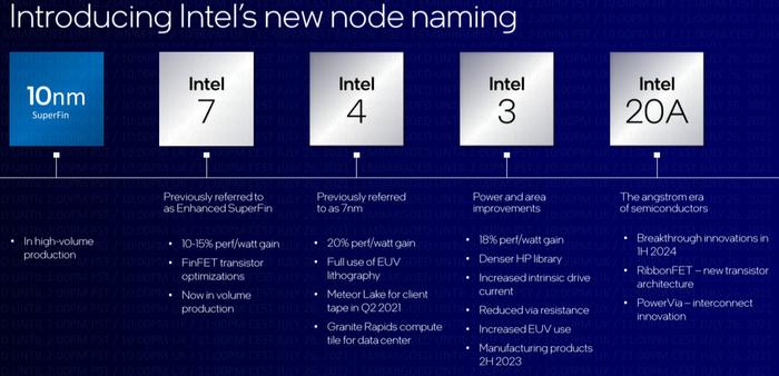
Without further ado, let us consider the new roadmap, embedded above (click to zoom in). On the far left, you can see where Intel is now, with 10nm SuperFin parts being mass-produced. In its recent earning statement, it said that its 10nm volume had surpassed 14nm ahead of schedule, so it is right to represent the current state with this node.
Intel's Enhanced 10nm SuperFin was going to come next, and the CPUs that were going to use this process were the first Alder Lake chips for laptops and desktops. Now, Alder Lake-P and -S chips will be described as 'Intel 7' processors. If you look at the chart you will see that Intel reaffirms that Intel 7 will deliver 10-15 per cent perf/watt gains, FinFET transistor optimisations, and are already in volume production.
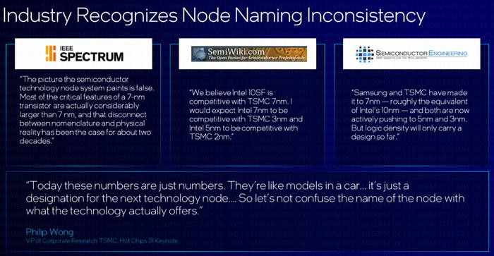
Intel supports its renaming scheme with quotes from semiconductor / scientific media
Moving further into the future, Intel 4 (previously Intel 7nm) will deliver a projected 20 per cent perf/watt gain, make full use of EUV, and the first Meteor Lake for client processors have already been taped in. Intel 3 continues, with greater density, increased EUV use, reduced via resistance, and you can expect to see Intel 3 products emerge during or after H2 2023.
Last but not least, on this roadmap, Intel expects to debut innovations based on the 'Intel 20A' process in H1 2024. The 'A' signifies the entering into the 'Angstrom Era' and if it had continued down the Xnm path it would have been called 2nm. In the video presentation, we heard that Intel already has engineers working on 18A processors for 2025.
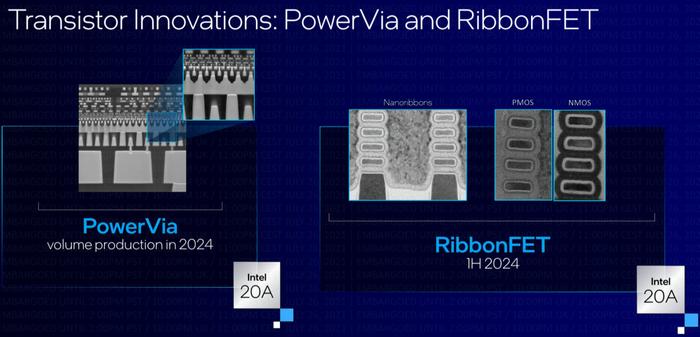
Another important thing happens when Intel reaches the Angstrom era. Transistor innovations such as RibbonFET and PowerVia should come into play. Transistor innovation is much more involved than making nodes smaller, chip designers and foundries can make use of other tech for higher densities and other optimisations. RibbonFET is the first new Intel transistor tech since FinFET and its nanoribbon structure features a gate wrapped around the channel. Intel says this allows for higher drive current at all voltages, for higher performance. PowerVia is Intel's implementation of backside power delivery, optimising signal transmission by eliminating the need for power routing on the front side of the wafer.
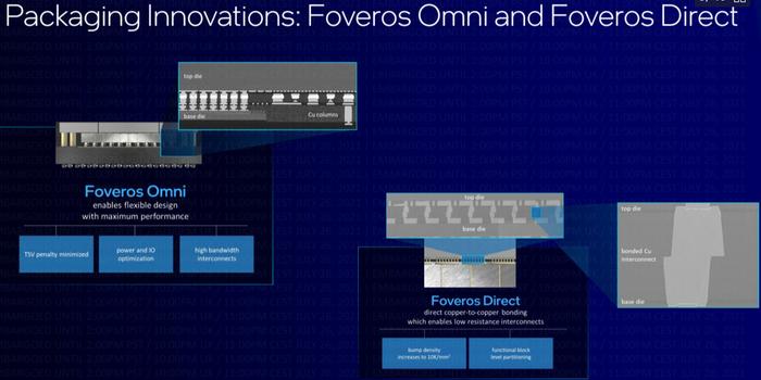
You have probably already heard of Intel Foveros 3D packaging technology. Now Intel has advanced it with Foveros Omni and Foveros Direct. Foveros Omni "allows die disaggregation, mixing multiple top die tiles with multiple base tiles across mixed fab nodes." Meanwhile, Foveros Direct enables sub-10-micron bump pitches and is claimed to blur the boundary between where the wafer ends and where the package begins.
In addition to the above tech news, Intel shared some of its recent IFS business successes. Qualcomm has signed up to fab some of its upcoming processor families on Intel 20A - which sounds like a big win. Amazon AWS will be using IFS for some of its server chip packaging duties too.


