


Reference Board Examination
VIA PT880 Pro Reference Board - VT8369A
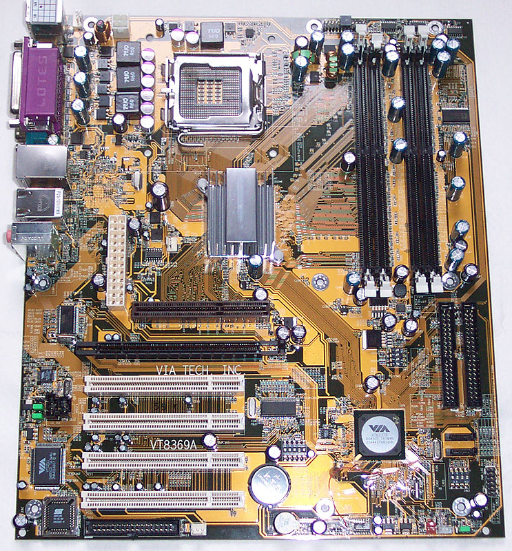
The reference board sports a VT8237R southbridge, DDR400 DIMM slots and LGA775, to partner the simultaneous AGP and PEG16X graphics slots.
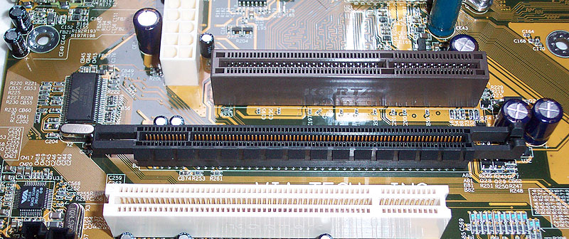
Getting the board up and running was a huge pain. Initially it wouldn't boot with either 1066MHz or 800MHz processors of any kind. Fearing the boards were dead (they'd failed initial testing in London), it took some trickery with the memory setup and PSU to get them up and running and passing POST before a new BIOS image could be flashed. The new BIOS had them running fine with 1066MHz processors which was my preferred bus speed of choice for testing but there were issues running pairs of graphics cards in the slots at the same time. Power seemed to be the reason why, high-end AGP and PCI Express graphics card pairs for testing the performance of the graphics interfaces simultaneously didn't want to work together.
A combination like GeForce 6200 (NV43-based) and GeForce FX5500 worked fine, two 6800 GTs would refuse co-operate. I'm hoping AIB partners place the slots further from each other than VIA did on the reference platform and implement the power circuitry correctly, for correct operation of a combination like that. Time contraints stopped me from doing much more than verifying that four-head was possible with two NVIDIA boards and I'll revisit that with final silicon and a partner board in due course.
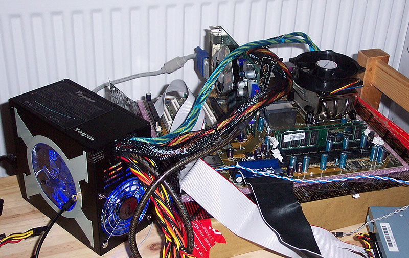
I won't mention the massive issues with board flex this time!
VIA PT894 Reference Board - VT5873B
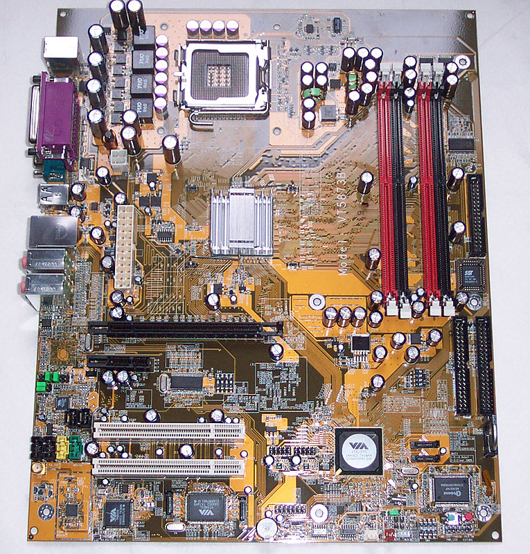
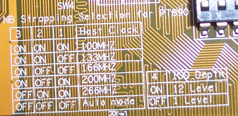
The PT894 suffered similar basic operating issues in the beginning; rather too much effort was required to get the board running well enough for testing. You can see the guide for DIP switch selection to let you choose basic front side bus clocks. If VIA are reading, your reference board programme has long been a little eccentric in terms of just getting basic benchmark results for an article. They need to be a little less queer in future.
There's very little to say about the layout of either board, such is VIA's willingness to break ATX layout rules (and there aren't that many to break!) and use as many ASICs from their range as possible in a reference board. You can assume that their AIB partner boards will look less like the result of a 'shroom session before operating the EDA tools for design.
I'm being hard on them, but it needs to be said.


