


What's new?
What better to help us understand a new chipset than with ye old Block Diagram.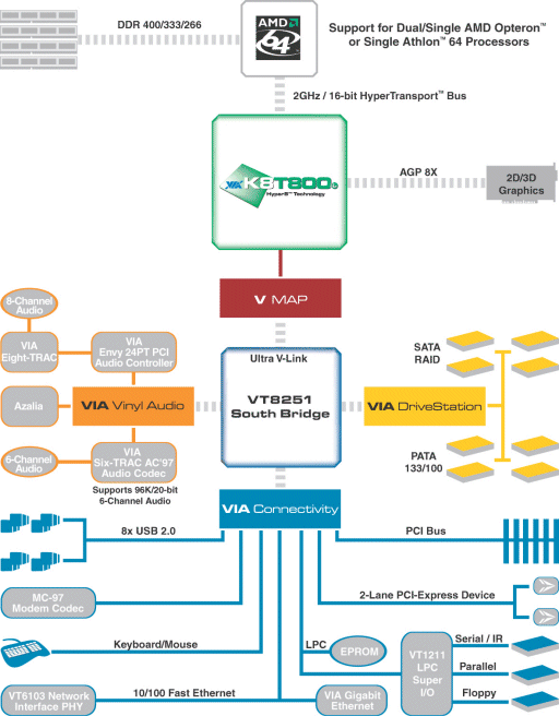
The block diagram applies equally to both S754 and S940 processors, and it will apply to S939 processors as soon as they become available. The first dotted line is an important one. It shows that memory considerations are taken away from the traditional CPU-to-northbridge route via (nice pun) a dedicated memory controller on the CPU itself. Depending upon the socket, that's either single- or dual-channel support at up to, presently, DDR400 speeds. NVIDIA's taken this opportunity to implement a single-chip design. VIA's continued with a two bridge approach.
The link between the CPU and northbridge, now widely known as the HyperTransport Bus, has been bumped up to 1GHz (2Ghz effective) from 800MHz. It's still a dual 16-bit-wide link, a feature that was native to only VIA until NVIDIA released the nForce3 250Gb. What's changed is the multiplier of the HT clock; it used to be 4X (4x 200MHz = 800MHz). It doesn't take a maths prodigy to work out that it's now 5X. In a single CPU setup, it's not of that much use for VIA, as the main bottleneck is created between bridges and not between CPU and Northbridge. For multiple CPUs, however, a faster link is of some benefit. Let's not forget that the chipset will service at least 3 different CPUs.
VIA's promoting the new VT8251 southbridge as a likely partner to the K8T800 Pro. That's not really the case at the moment. As you'll see in a moment, the reference board simply uses the established VT8237. We doubt whether initial retail boards will offer anything different. '8251 will probably see the light of day some time in the summer, so it's inclusion in a block diagram is just a forward-looking measure. To bring this point home, VIA's current K8T800 Pro block diagram, found here, reverts back to showing the good ol' VT8237. VIA's also keen to point out the 1066MB/s Ultra V-Link bridge interconnect on the K8T800 Pro. It's a wise move when one considers the amount of bandwidth a number of high-speed controllers can chew up concurrently.
What the above diagram also fails to highlight is something that's been on enthusiasts' lips for some time. The initial K8T800, whilst being a decent enough, ran AGP and PCI buses in relation to the HT clock. Increase one and the others have to increase, too. What VIA's done is to have both sensitive buses run asynchronously, such that they can be explicitly locked should the need arise. Consider running an Athlon FX-51 at, say, 2420MHz. That's 11x220MHz in oveclockers' language. Try running PCI-based (Silicon Image's range springs to mind) SATA controllers and associated hard drives at that speed for any length of time. In short, asynchronous, locked buses are an absolute must if one wants to try anything much above stock speeds. Intel's managed it on its dual-channel chipsets for some time, so it's about time that NVIDIA and VIA did the same for S940/754.
Other than a faster HT clock and ability to lock buses, there's not too much new for VIA to shout about. The upside of this is that manufacturers can simply slot in the new bridges without too much fuss, especially with VIA's handy VMAP architecture. It's then difficult to see how exactly the Pro will fit in. Will there be a revision 1.0 featuring the present VT8237 southbridge and another with the above-described VT8251?. Our educated guess is that a few manufacturers will jump on to the K8T800 Pro bandwagon at the earliest possible instance. Others will wait a short while whilst VIA can supply the VT8251 southbridge, decked out with on-chip Gigabit Ethernet and support for PCI-Express. Buyers will need to examine specifications carefully to know exactly what they're buying into.


