|
The original chipset was made up of a pair of chips, the IGP-128 or SPP-128 and the MCP. The IGP-128 or Integrated Graphics Processor was the version of the nForce northbridge with the GeForce2 MX graphics core on board (420). The SPP-128 was the coreless version (415). The MCP was the southbridge and contained the APU and the rest of the southbridge based technologies.
This revised chipset is made up of the IGP-128/333 or SPP-128/333 and the MCP. The functions of both IGP and SPP remain the same as before but the 333 parts of the names hint at what's new in nForce2 and what makes up the core of the new chipset update.
333MHz busses ahoy
333 in the names of the northbridges here reflects the official support for both 333MHz front side bus Athlon XP's (yep, they do exist, check out my other review today for details) and 333MHz memory. 333MHz in both cases represents a DDR bus clocked at 166MHz where data is transferred on both the rising and falling edges of the clock signal.
So we have 333MHz support in two areas and all that entails. In terms of CPU-to-bridge bandwidth, that goes up to 2.7GB/sec from the 2.1GB/sec you'll find in current 266MHz bus supporting chipsets. In terms of CPU-to-memory bandwidth, that goes up to a staggering 5.4GB/sec, the highest memory bandwidth of any current home PC, consumer based chipset. It achieves the figure by implementing a pair of memory controllers within the new bridges and they operate side by side at 2.7GB/sec (in 333MHz memory bus mode) for a total of 5.4GB/sec.
It's a well known fact that if the CPU can only make use of 2.7GB/sec, memory bandwidth in excess of that wont be used. That's very true, but other components in the nForce2 package are designed to be able to access main memory without the need for the CPU, working independently of the CPU to achieve max performance. The MCP is able to address main system memory without the help of the CPU so the extra 2.7GB/sec provided by the memory controller in TwinBank mode becomes useful. As far as I'm aware, no other shipping Socket A chipset for the AMD platform can do such a thing. While it's still a lot of extra bandwidth and due to the processor design it will never full be utilised, even with CPU in full bandwidth hogging mode since the MCP can't create 2.7GB/sec of traffic to the memory controller. But due to the design of a pair of memory controllers, 5.4GB/sec is what you get and it's certainly a healthy number and at least some of it will see some usage under load.
The chipset also supports a massive range of memory multipliers to run the memory bus faster or slower asynchronously from the processor bus. NVIDIA is also touting DDR400 support mainly via a 120% multiplier at 166MHz (333MHz) processor clock and the resulting 6.4GB/sec that gives the system. 120% isn't the only memory multiplier available tho and DDR400 support is also available at 133MHz (266MHz) processor clock for 6.4GB/sec with a 2.1GB/sec processor. A bit of a mismatch and no real performance increase at all over say 333MHz memory at 133Mhz cpu clock but NVIDIA are pushing DDR400 support so I better mention it.
AGP8X support
So on the new IGP/SPP, we have support for 333MHz technologies and all the lovely new bandwidth that that brings to the table. Another bandwidth increase can be found in the form of the AGP8X controller on both bridges. This is one of the reasons why the chipset has take so long to arrive at market along with the official support for the new Athlon XP's. AGP8X products are only just starting to arrive and NVIDIA are only just about to release their own. Support for AGP8X was one of NVIDIA's design goals for this chipset and they needed to test with AGP8X products. AGP8X increases controller bandwidth to ~2.1GB/sec from ~1.06GB/sec. In some original NDA documents that I got back in April that outlined the new nForce solution, AGP8X isn't mentioned so it's an addition to the chipset that had to be engineered in.
Still only APU v1.0
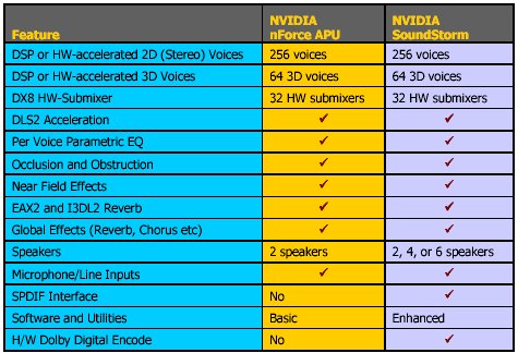
A lot of people will be expecting an update to the APU, the audio process that's part of the MCP. Unfortunately it's still the same old revision 1.0 APU that we saw in original nForce but that's not necessarily a bad thing. The original APU was very highly specced in terms of audio performance. A full hardware Dolby Digital 5.1 processor, full hardware DirectX 8.0 support, 256 hardware voices and a full digital output interface that could do AC3 steam processing in hardware made it the most powerful on board audio solution for a personal computer.
All that stays in nForce2 except it's configured slightly differently so that NVIDIA can market it on 2 levels.
SoundStorm
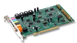
SoundStorm is basically a partitioning of the technologies available on the audio side of the MCP. Basic boards without a SoundStorm add-in board (on the test setup, it was an ACR card but there's nothing stopping it being a PCI board) will only have access to a subset of the features available on the MCP. SoundStorm equipped solutions get everything. Here's how it pans out with a quick pic of the ACR card (stolen mercilessly from an NDA'd PDF, no good cam shots of the test system I'm afraid, see the XP2700+ review for lovely nForce2 shots however, and no press images of SoundStorm are around).
Everything else
The MCP also gets a worthy feature bump just like VIA's VT8235 southbridge. There are actually 2 versions of the MCP, the MCP and MCP-T. MCP-T is a super set of MCP so I'll cover the MCP features first and then the extras in the T version.
The new MCP features current technologies like a 6 port single USB 2.0 controller for hooking up your high speed USB devices. No USB 1.1 support as such, just backward compatibility with the old spec in the new controller.
You also get an update of the integrated Ethernet controller that features SteamThru, another NVIDIA technology. StreamThru can talk over the HyperTransport bus to the CPU independantly of the other MCP components, running isynchronously. This lets the Ethernet controller communicate with the CPU at maximum effeciency. It's still a 10/100MBit solution, no Gigabit version yet.
You now get a pair of ATA133 controllers on MCP as opposed to the single controller on the original.
MCP-T takes things a step further with support for IEEE-1394a or what's more commonly known as Firewire. Another high speed serial bus like USB 2.0, it generally supports a different class of device to USB 2.0 and both are pretty commonplace on new systems so they make an appearance here.
Lastly on top of the new MCP features, MCP-T also has a 3Com Ethernet controller for dual-NIC capabilities. I'm not entirely sure why they didn't build a second NVIDIA controller onto MCP-T but a 3Com controller is there and NVIDIA calls this DualNet. How original! A nice configuration for those situations where two NIC's are handy like running Ethernet based broadband and a seperate internal network. You can do this on MCP-T based boards out of the box (providing you get the headers).
In a nutshell
So what you are basically looking at over original nForce is support for new 333Mhz bus Athlon XP's, support for DDR333/DDR400 memory at 133 and 166MHz cpu clock, the same APU with all its audio goodness and a bang up to date set of southbridge features like Firewire and USB 2.0. DualNet is worth a mention too.
A healthy upgrade of the MCP, the best memory controller on Socket A and also a new graphics core. I haven't mentioned the GeForce4 MX graphics core on the IGP-128/333 for the simple reason that neither nForce2 solution at Hexus bore the IGP, rather the SPP on both boards.
GeForce4 MX for those that are interested supports 24 of the 26 pixel shader functions in DirectX 8.0/8.1 so it's not a true DX8 hardware accelerator (something ATi love to shout about) but it's still respectable for an onboard solution.
Sorry I can't cover it in more detail just now, we will when we get a board that features it.
If you want to know what TwinBank and the DASP techs are, have a peek at my MSI K7N420 Pro featuring the original nForce chipset. Things are still the same and still present, just with support for new memory speeds.
Lets take a look at NVIDIA's reference board to see how they've done things with their reference implementation.
|