


FX 5700 Ultra
I get the pleasure of looking at the Ultra versions of both boards today and it's FX 5700 Ultra first. 9600XT's new nemesis, it's a twist on 5600, with a fair few enhancements.According to NVIDIA, 5700 (NV36) is a completely new design and not just a speed bumped 5600. With a claimed 3 times the vertex processing power than 5600 at the same clocks, something impossible to claim without a silicon overhaul, it appears on the surface to give NVIDIA a decent mid-range contender.
NV36 also marks a first for NVIDIA in that it's the first GPU produced with assistance from IBM. Whether that extends any further than simple manufacturing production of the GPU design, I can't confirm, but NV36 is built using IBM's 130nm process technology. I've heard rumour that IBM wont produce NV36 exclusively, that TSMC (NVIDIA are their largest customer) will be producing NV36 GPU's too, but I can't confirm that either. I'll leave that to sites with more PR cattle to prod than I do.
As far as technical specs go, 5700 looks like 59xx with half the pixel pipelines and a 128-bit memory interface.
Sharing Intellisample HCT, Ultrashadow and the CineFX 2.0 hardware, it's functionally equivalent to 59xx in every way, looking for all the world like a 4-pipe NV35.
Here's the table of numbers, along with those of its direct competitor.
| GeForce FX 5700 Ultra | Radeon 9600XT | |
| GPU Name | NV36 | RV360 |
| Transistor count | Unknown | Unknown |
| Manufacturing process | 130 nanometre | 130 nanometre |
| Pixel pipelines | 4 | 4 |
| Pixel shader units | 1 per pipe | 1 per pipe |
| Memory bus width | 128-bit/16-byte | 128-bit/16-byte |
| Texturing units | 1 per pipe | 1 per pipe |
| Core clock | 475MHz | 500MHz |
| Memory clock | 906MHz DDR | 600MHz DDR |
| Pixel fillrate | 1900 Mpixels/sec | 2000 Mpixels/sec |
| Texture fillrate | 1900 Mtexels/sec | 2000 Mtexels/sec |
| Memory bandwidth | ~14.40GB/sec | ~9.60GB/sec |
So with nearly identical core clock speed and a significantly larger chunk of memory bandwidth compared to 9600XT, IBM's process trickery, all the NV35 Intellisample (Z-buffer, antialiasing, texture filtering) smarts and a claimed 1.5x increase in overall performance over the outgoing 5600, it looks like something nice for new mid-range customers. What about a physical implementation in the form of the reference board?
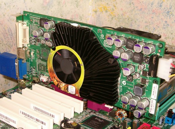
Sat in the test rig (excuse my floral wallpaper), it's the same width as an FX5900 board. You can see it's got a single slot cooler design which should be adopted (at least in the number of slots needed) by retail board vendors. It also needs external power from a standard 4-pin power connector and I'm assured that a splitter will ship with all retail samples.
Underneath the cooler, removal of which was very simple, sits the new GPU, manufactured by IBM.
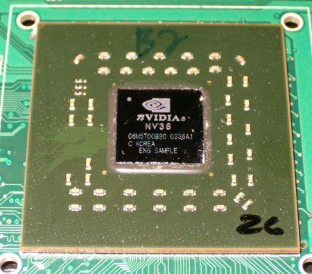
Cleaned up a little to remove the remnants of the thermal pad (this happened after all benchmarking was completed, so as not to influence results in any way), it looks for all the world like a desktop CPU without a socket to sit in. Soldered directly to the PCB with no heatspreader (unlike the current 5600 and 5900 series), its core is cooled directly by any heatsink device.
Memory is Samsung's K4N26323AE GDDR2, the GC22 variant. A 128Mbit GDDR2 device, specced for operation at 450MHz (900MHz DDR), it runs at full speed on 5700 Ultra's.
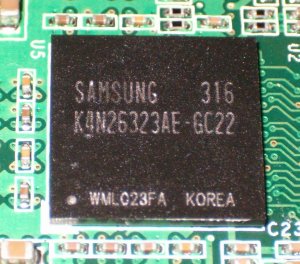
With 4 chips per side, each 128Mbit (4Mx32), we get a total of 128MB of framebuffer memory for use by the GPU. The memory interface, a 2 crossbar 128-bit dual channel implementation that appears to be identical to the interface used on NV35, it gives a maximum theoretical bandwidth of 14.4GB/sec. Being a crossbar design, memory accesses can occur on 64-bit or 128-bit data boundaries, offering performance increases over a single interface design, where data access must occur when 128-bit of data is ready to be read or written.
The reference board is a simple dual head design with TV-out, with DVI-I, analogue DSUB and 4-pin S-Video outputs that may drive a total of 2 displays. NVIDIA's nView2 software controls the implementation, which remains unchanged compared to the outgoing GPU's. Of coure board makers are free to equip 5700 boards with VIVO chips for video input processing, so look out for boards with that from the likes of Gainward and MSI.
Back view
NV36 product designation sticker, denoting A1 silicon revision
What about FX 5950 Ultra?


