


Architecture discussion
GeForce GTX 580 - high-end Fermi done right this timeGeForce GTX 580 is a GPU that's born to right the inadequacies of GTX 480, then. The architecture is ostensibly the same, based on Fermi, but NVIDIA's engineers have gone back to the drawing board and modified the design for better performance. This table highlights the key derivations and compares GTX 580 to incumbent GTX 480 and 470.
| GPU | NVIDIA GeForce GTX 580 1,536MB | NVIDIA GeForce GTX 480 1,536MB | NVIDIA GeForce GTX 470 1,280MB |
|---|---|---|---|
| Transistors | 3.0bn | 3.0bn | 3.0bn |
| Die size | 520mm² | 529mm² | 529mm² |
| Fermi revision | GF110 | GF100 | GF100 |
| General clock | 772MHz | 700MHz | 607MHz |
| Shader clock | 1,544MHz | 1,401MHz | 1,215MHz |
| Memory clock | 4,008MHz | 3,696MHz | 3,206MHz |
| Memory interface | 384-bit, 1,536MB GDDR5 | 384-bit, 1,536MB GDDR5 | 320-bit, 1,280MB GDDR5 |
| Memory bandwidth | 192.4GB/s | 177.4GB/s | 133.9GB/s |
| Shaders | 512 | 480 | 448 |
| GFLOPS | 1,581 | 1,345 | 1,089 |
| Texturing | 64ppc
bilinear 64ppc FP16 |
60ppc
bilinear 30ppc FP16 |
56ppc
bilinear 28ppc FP16 |
| ROPs | 48 |
48 |
40 |
| ROP rate | 37.1 |
33.6 |
24.28 |
| GTexel/s bilinear | 49.4 |
42 |
33.99 |
| FP16 rate | 49.4 |
21 |
17 |
| Board power (TDP) | 244W | 250W | 215W |
| HDMI | 1.4a | 1.4a | 1.4a |
| Retail price | £399 | £340 |
£190 |
The same...but different
Look through the numbers and, really, the GeForce GTX 580 can be thought of as largely similar to GTX 480. Both GPUs share a basic topology that's manifested in a high-level overview which looks like this:
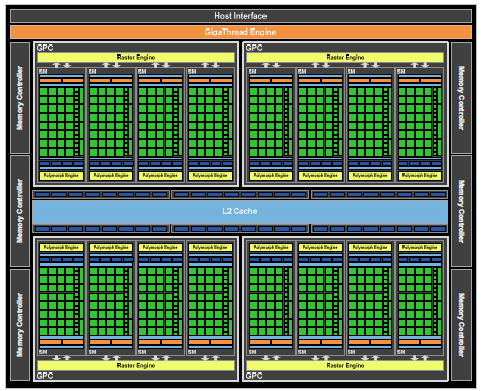
GF100 and GF110
This is GF100 in all its glory. This is also GF110 (GTX 580) in all its glory. The differences between the two high-end Fermis requires some drilling down.
NVIDIA has variations of the Fermi architecture for different pricing segments. The high-end part is referred to as GF100, the mid-range as GF104, and the lower-end of the spectrum as GF108. The newer dies aren't simply cut-down versions of GF100. For example, GF104 - that's GeForce GTX 460 to you and me - has half as many streaming multiprocessor (SM) units as GF100 but, crucially, each SM has 50 per cent more cores - 48 vs. 32 - and a 100 per cent increase in texture units - eight vs. four - and special-function units.
512-core model
Thinking along these lines, the GeForce GTX 580's GF110 core is more than just a rebranded GF100. First off, NVIDIA finally uses the full allocation of 16 PolyMorph engines and SMs for GTX 580. With 32 cores per SM, we have a GPU-wide tally of 512, representing a full Fermi chip. Remember that GTX 480 has an SM turned off, leading to 480 cores. Ceteris paribus, under ideal conditions, this gives GTX 580 an additional 6.7 per cent of power.
FP16 speed improvement; better z-cull
But NVIDIA goes a little further than just boosting the geometry and core count. Each SM unit is still comprised of four texture units, meaning a card-wide 64. This time around, each unit can filter a floating-point 16-bit (FP16) texture in one clock cycle, as opposed to two on all other GTX 400-series cards. This means the GTX 580 is faster for filtering in scenarios where high-dynamic range rendering is copiously used. Keeping our improvement ticker going, add on a few per cent extra performance over same-clocked GTX 480 for games that use HDR.
GTX 580 also has an improved z-cull feature, where pixels that won't be seen by the viewer are discarded from being processed. The GPU does this by calculating the depth of the pixel, that is, if it is going to be rendered behind other on-screen geometry.
Mega Hurts
Some performance will be added by the extra cores and associated PolyMorph engine, some will come from running FP16 at full chat. The bulk of the gains arrive from higher clocks. Look back at the table and you will see that GTX 580 ships with a 772MHz core speed, 1,544MHz shader, and an effective memory clocking of 4,008MHz. Simple math tells us that GTX 580 will be between eight-to-10 per cent faster than GTX 480 through higher clocks alone. Indeed, the frequencies are a slap in the face for current pre-overclocked GTX 480s; partners better get shot of them pronto.
The four main performance-related improvements of GTX 580 - more cores; full-speed FP16; better z-clear, and higher clocks - will, we reckon, give the new GPU a 10-25 per cent advantage over the current single-GPU champ, with the improvement based on just how partial the gaming title is to architectural refinements.
Now the question is how has NVIDIA given you more speed with a similar power rating? We're glad you asked.
Containing the power
GTX 480 is one hot-running beastie. Give it some FurMark love and watch the watts spiral out of control, way above the rated 250W TDP, and hear the reference cooler's fan run fast enough to sound like a turbine. The cooler's deficiencies have been well-documented in the press. NVIDIA doesn't like you running FurMark, mainly because it's not indicative of real-world gameplay and causes the GPU to run out of specification. We like it because it makes high-end cards squeal!

So concerned is NVIDIA with the pathological nature of FurMark and other stress-testing apps, it is putting a stop to it by incorporating hardware-monitoring chips on the PCB. Their job is to ensure that the TDP of the card isn't breached by such apps, and they do this by monitoring the load on each 12V rail.
Should a specific application hammer the GPU to the point where the power-draw is way past specification, as FurMark does to a GTX 480, the hardware chips will simply clock the card down. Pragmatically, running FurMark v1.8.2 on the GTX 580 results in half the frame-rate (and 75 per cent of the load) that we experience on a '480 with the same driver. The important point is that the power management is controlled by a combination of software driver and hardware monitoring chips.
NVIDIA goes about the power-management game sensibly, because the TDP cap only comes into play when the driver and chips determine that a stress-testing app is being used - currently limited to FurMark v1.8+ and OCCT - so users wishing to overclock the card and play real-world games are able to run past the TDP without the GPU throttling down. Should new thermal stress-testing apps be discovered, NVIDIA will invoke power capping for them with a driver update.
In effect, high-end NVIDIA's GPUs are being safeguarded against the noisome problems associated with leaving GPU-bustin' apps running for significant periods of time. There's no way around this from now on, folks, because NVIDIA won't enable end-user control over power capping.
NVIDIA says that it has re-architected large portions of the GPU for better power-draw characteristics. Using a combination of lower leakage and higher speed transistors in critical portions of the GPU, the modifications enable the GTX 580 to ship with a slightly lower TDP compared to the slower GTX 480. Had the GTX 480 simply been overclocked to these new speeds and the extra cores made available, we doubt that it would have shipped with a sub-300W TDP rating.
Round it up
GeForce GTX 580 is better than the incumbent GTX 480 in four main ways: a) it's clocked in at higher frequencies b) it has more 32 extra cores and one additional PolyMorph engine c) FP16 (bilinear) filtering now runs at twice the speed d) design improvements mean a lower TDP for a faster GPU.
These improvement are enough, NVIDIA thinks, to change the naming scheme. We reckon it should have been called the GeForce GTX 490, but then again, AMD also indulges in some model-number inflation. Enough words; let's see some more pictures.


