


Radeon X8-series Crossfire Edition
Radeon X8-series Crossfire Edition boards all look the same (as far as HEXUS are aware), with the same PCB and cooler, regardless of whether it's the 256MiB Radeon X850 Crossfire Edition (Radeon X850 XT basic configuration), 256MiB Radeon X800 Crossfire Edition (Radeon X800 XL basic configuration) or 128MiB Radeon X800 Crossfire Edition (Radeon X800 XL clocks, 128MiB of memory).The PCB design and cooler are shared for obvious reasons, keeping the costs of creating a new PCB design that can accomodate the compositing chip and associated output hardware down since there's just one. The 256MiB boards have memory devices on both sides of the PCB, 128MiB boards house them on the front only.
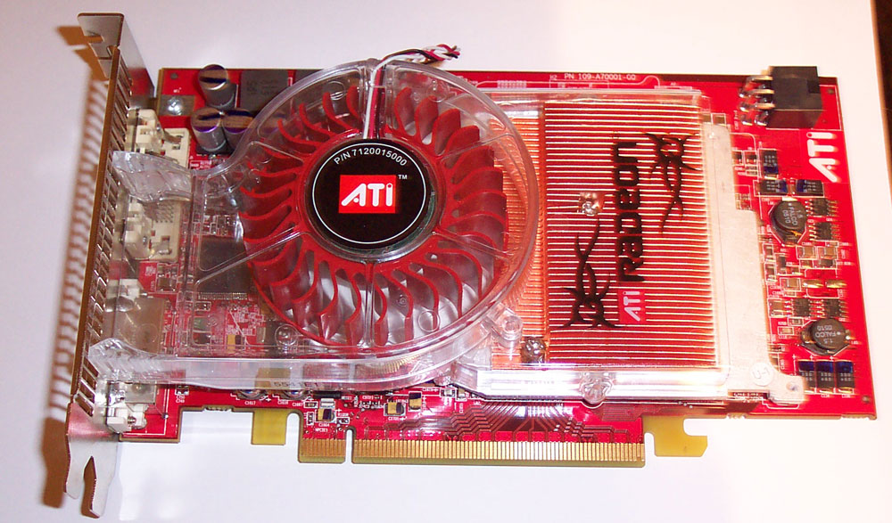

As you can see from the front of the pictured ATI Radeon X800 XL Crossfire master board, the cooler ATI use for the GPU (R430 in this case) and the memory devices (2.0ns GDDR3 from Samsung) is the dual-slot cooler first seen on the Radeon X850 XT Platinum Edition. The cooler draws air over the GPU heatsink from your case and exhausts it out via the gaps in the card's backplane space, above the DVI and DMS-59 high density connector.
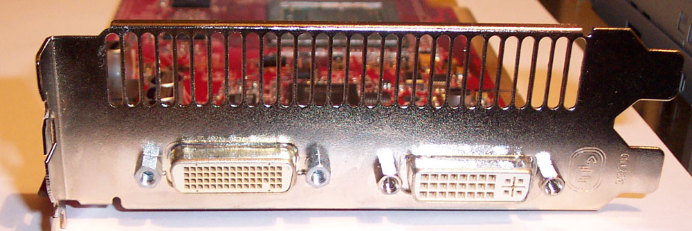
From the rear it's not obvious you're looking at a Crossfire board, bar the sticker underneath the retention plate which also cools the rear memory modules. The backplane shot shows the DMS-59 connector and the usual DVI display output. The incoming signal from the slave comes across the Crossfire cable and into the compositor via the DMS-59.
The naked board shot shows the compositing chip and its supporting output hardware.
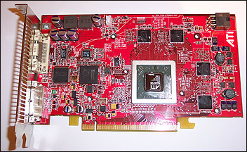
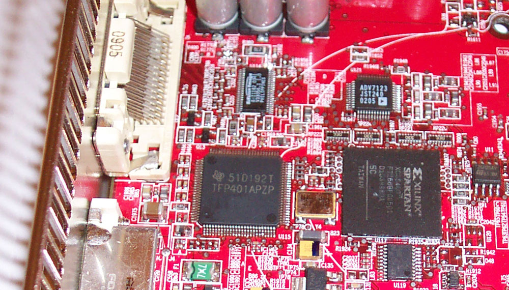
Look closely at the board and you can see the compositing chip (the largest black chip in the linked picture). ATI use a programmable FPGA from Xilinx (a Spartan 3 XC3S400 with 400,000 gates and 36KiB of memory to work with) to implement the compositing logic needed to put frames together before output.
If you look at that area of the board again, you can see there's also a Texas Instruments TFP401A-PZP single-link DVI receiver for accepting the frame input from the slave board. That's then processed by the XC3S400 programmed with ATI's compositing logic before being spat out via an Analog Devices AD7123 10-bit DAC (for analogue output) and Silicon Image Sil1162 single-link DVI TMDS transmitter (for digital output). So frames come into the Ti, are processed by the Xilinx which is being fed by the master's DVO port, before combined frames are spat out via the Analog Devices DAC and the Silicon Image TMDS.
The DVI output is fed by the GPU's on-chip single-link TMDS transmitter. And that's about it as far as the Crossfire Edition X8-series boards go. They're PCI Express (obviously) and require a power feed from your power supply to run properly. Neglect to connect a 6-pin PCI Express power connector to an X8-series Crossfire master board and sonic hell breaks loose to remind you to connect one up immediately, lest your eardrums collapse and you black out. Only joking, but it's best you remember that if you're building your own Crossfire system, O.K. ?
"Vot about ze Crossfire mainboards for AMD and Intel, Direktor Rys", I hear you all cry. "Turn ze page, comrades", I reply.


