


Reference Board Examination
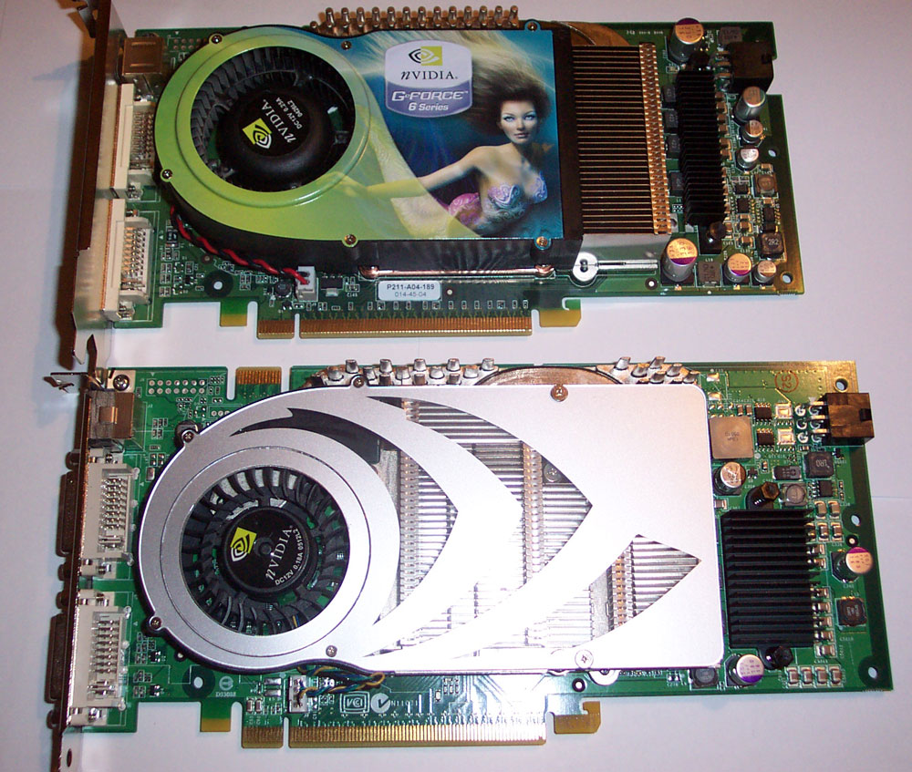
Behold! G70 twofold, in the form of a pair of GeForce 7800 GTXs. Click all the images on this page for bigger ones, 1000 pixels wide.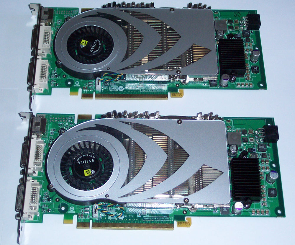
With SLI all the rage, reference boards from NVIDIA these days come as identical twins. The 7800 GTX has a few obvious talking points, so if you want to pull up a chair and have a good look at one on its own, I'll give you the grand tour.
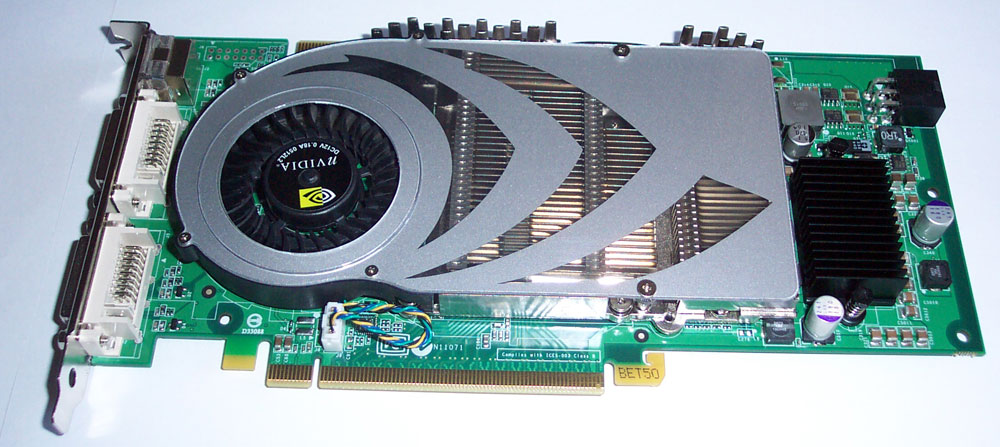
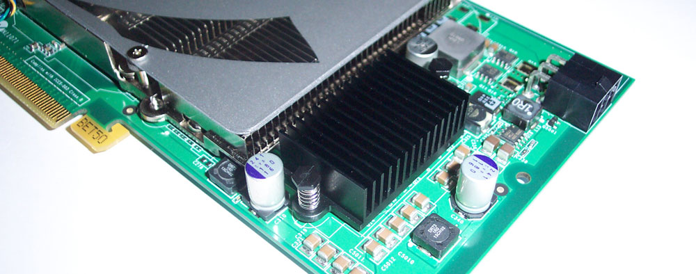
Longer than a 256MiB 6800 Ultra or 6800 GT, the PCB for the 7800 GTX isn't small. Without one to hand, I'd say it's just shorter than the 512MiB 6800 Ultra that various vendors have been peddling (where are the review samples, boys?) in recent times. The single-slot aluminium reference cooler causes the board to weigh in at around the same 320g as a reference 6800 GT, and a fair bit less than a reference 6800 Ultra.
Single-slot is one of the key indicators to a faster flasghip product, probably labelled Ultra, which will likely sport a dual-slot cooler. Hilariously, NVIDIA used really tiny Philips screws to retain the heatsink's branding plate. Without the aid of my watchmaker's screwdrivers, which seem to have perished in my recent house move, I've not been able to have a peek underneath to show you the GPU itself. Twenty quid says Wasson or Baumann did, though.
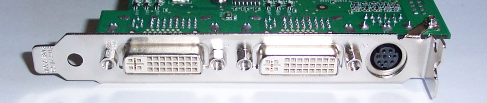
The cooler hides the dual-link TMDS that drives the first of two DVI ports. The dual-link TMDS can drive larger digital displays than the single-link (1600x1200) DVI links on almost all other NVIDIA boards made to date. Indeed, the panel that the linked Ultra DDL was designed to drive is one such beast that the 7800 GTX can make light work of.
Notice how NVIDIA use digital VRMs this time, for power management; there's barely three capacitors on the entire product. A black aluminium heatsink cools a FET bank whos high switching speeds equals heat to manage. Being PCI Express, there's ~75W available from the slot (see the first few pins on the connector? they're for power) with a 6-pin power connector giving the board the rest.
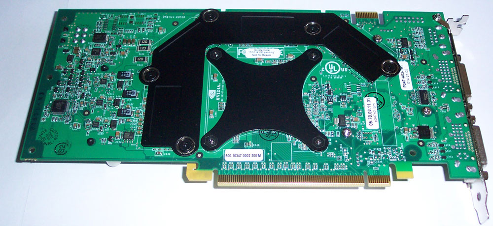
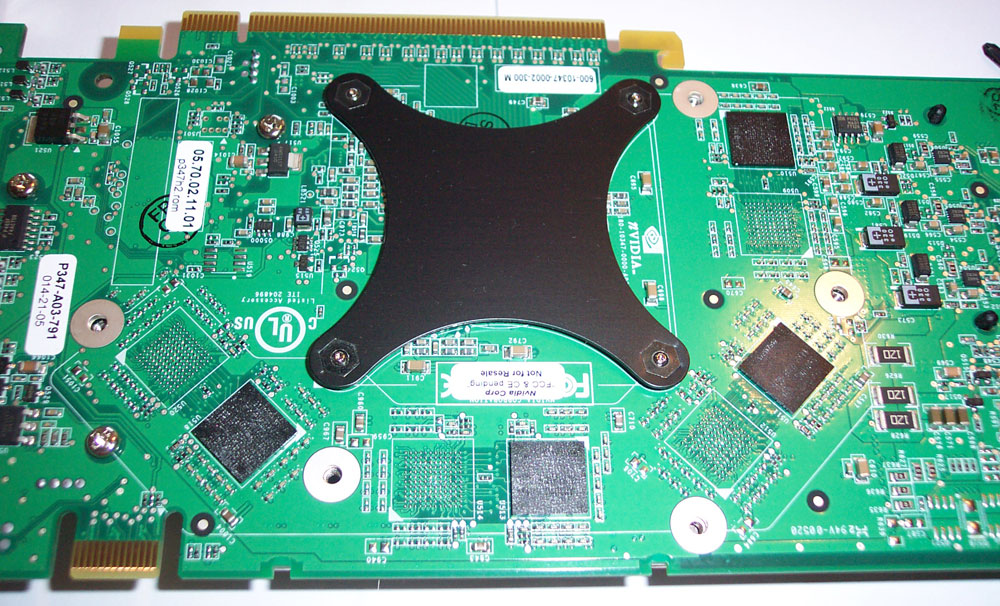
The rear of the board shows you how the GPU is positioned centrally with its heatsink retained by a fairly sizeable bracket. Another bracket, L-shaped, covers the rear memory modules and double up as a retention mechanism for the rest of the cooler. Exposed, you can see four of the eight GC16, 600MHz (1200MHz DDR) Samsung GDDR3 DRAMs that have been ubiquitous on high-end graphics hardware for the last, ooh, 14 months. They're the same chips that powered 6800 Ultra and they show up here, too.
With four DRAMs on the front of the PCB and four on the back, with obvious room for eight more, 512MiB boards (or 1GiB should NVIDIA prise double-density DRAMs from Samsung's mitts) should show up in due course. Another clue we're missing an Ultra with a fat framebuffer?
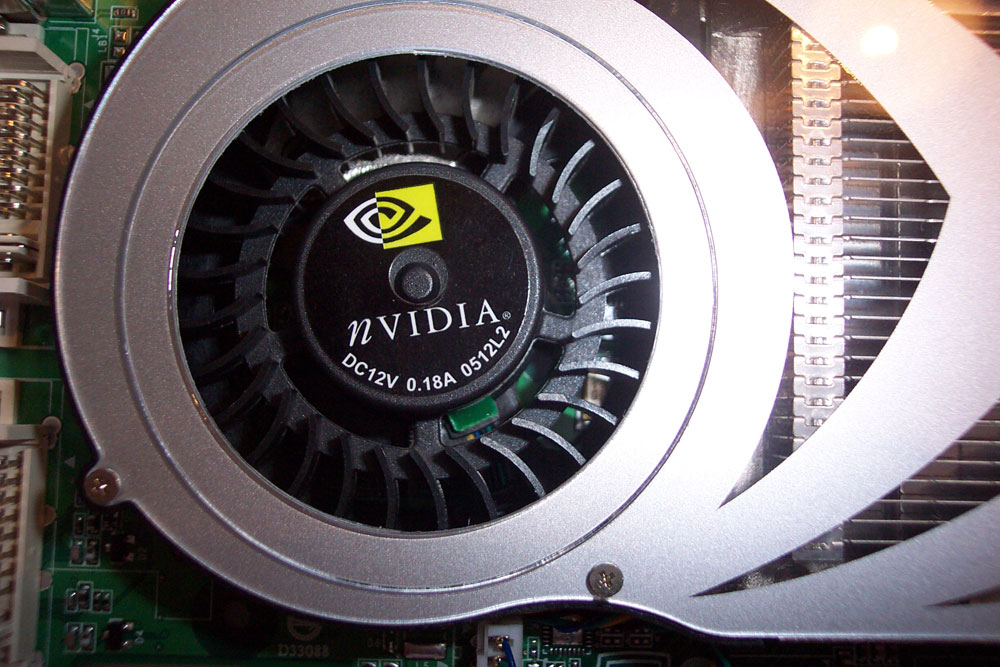
It seems to have a 1.25V Vcore voltage for the 430MHz core clock (I hate prodding unreleased hardware with meters to check properly), and going by the lack of noise the cooler makes under all but the heaviest of loads, it doesn't get too hot. That's not to say that at full chat they aren't loud - they really are, and with two on the go for SLI you definitely hear the noise they make - it's just that the temperature-controlled fans didn't seem to hit full chat all that often. As always, your chassis cooling helps immensely in that respect.
Power wise, NVIDIA will tell you that a single board draws 100W under load and two boards in tandem need 220W. That's pretty close to the mark, with my calculations showing an extra 80W or so of output power consumed when you add in a second board.
NVIDIA claim that a 500W power supply is needed for SLI running. That's an overstatement, designed to protect them from craptastic supplies that can't supply the output power an SLI system needs. If there's any more than a 300W output power from a high-end SLI rig with GTXs (without loading it up with disks), I'll be very surprised. 100W is less than 9 amps from a 12V source. Any decent ATX or ATX2.0 can pull 18A with room to spare for the CPU, and with ATX2.0 you've got that from an independant voltage rail. Just make sure your power supply is from a decent, trusted vendor, and you'll be fine. I used a Tagan TG480-U01 during all my testing, including SLI and with the most powerful x86 processor on the planet, without any issues.
The board exam done and dusted, let's see how the board does in terms of image quality and all important performance.
Addendum: Die shot and DRAMs
Since the publication of the article I've managed to take the clothes off of a reference 7800 GTX, in the name of watercooling. The large die is visible in the following photograph.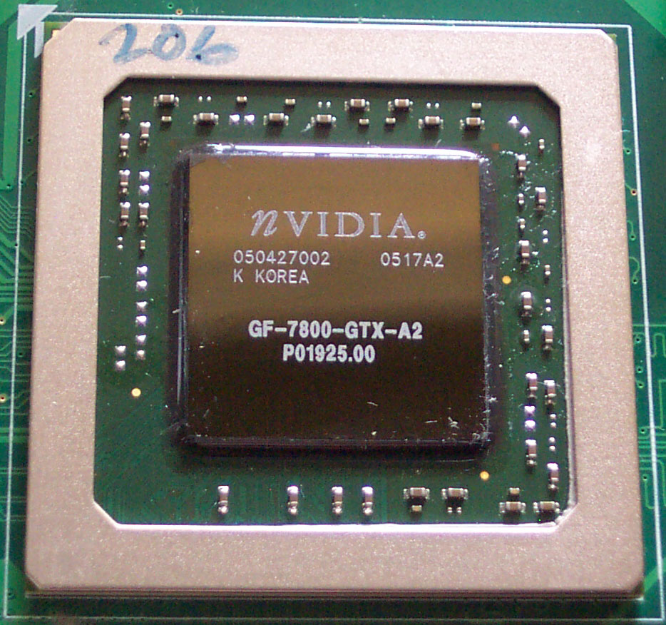
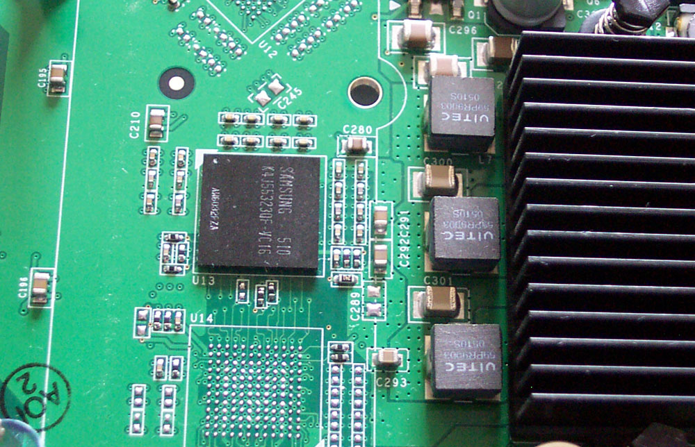
A week 17, 2005 example (sometime in May), that particular G70 die is marked specifically for production of the GeForce 7800 GTX SKU. The DRAMs are Samsung K4J55323F VC16 parts, not GC16 as I reported above. The V designation means it's the lead-free variant of the 1.6ns part.


