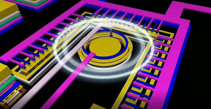
A long sought after goal in optics and electronics has been reached thanks to the work of researchers at the University of Twente (UT) in Enschede, Netherlands. In brief, as explained by the UT news blog, for the first time researchers have been able to connect two parts of an electronics chip "using an on-chip optical link". Previously conventional silicon CMOS tech wasn't able to be used to fabricate such a chip so the deployment of 'bulky' optocouplers was required. Conversely, the new UT optocoupler is about 0.008 square millimetres in size and consumes minimal energy as integrated into a CMOS chip.
Two worlds collide
The UT blog provides some interesting background to the CMOS optocoupler achievement which enables on-chip optical links. Apparently silicon is a poor material for LED light sources as it is low efficiency and the light emitted is mainly in the IR spectrum. On the other side of the equation a silicon detector doesn't work well with IR light sources... A key technique discovered by the UT researchers was to connect the silicon LED 'the wrong way', which would cause an 'avalanche effect' resulting in the emission of visible light.
On-chip optocoupler interview from University of Twente on Vimeo.
In his PhD thesis Vishal Agarwal from UT shares his design for an optocoupler that can be fully integrated in CMOS, with a data rate of about 1 Megabit per second and minimum energy consumption. It is claimed that this is an acceptable data rate for many applications – like smart power chips which isolate certain chip areas using light-only communications. However, data rates would be able to be "increased at least tenfold," according to Agarwal.