


0

AMD DETAILS GROUNDBREAKING RESEARCH IN NEW TRANSISTOR AND MEMORY CELL STRUCTURES
|
Quick Link: HEXUS.net/qab7c
Add to My Vault:
|
|
-Breakthroughs presented at IEDM 2002 could serve as the foundation for future, higher-value customer solutions-
SUNNYVALE, CA. - DEC. 9, 2002 - Demonstrating its leadership in semiconductor research and development (R&D), AMD will present several new technical achievements critical to the creation of next-generation transistors and memory cells at this year's International Electron Devices Meeting (IEDM) held in San Francisco, December 8-11. Aspects of the research may be used in products as early as 2005.
"AMD labs are already well into development of next generation transistor and memory technologies that, once perfected, will power our customers' products to unprecedented levels of performance, connectivity and ease-of-use," said Craig Sander, vice president of process technology development at AMD.
Next-Generation Transistors
At IEDM, AMD will present three technical papers outlining recent achievements in their ongoing research on future transistor structures. The primary working parts of a microchip, transistors are basically a microscopic switch that uses a "gate" to turn the flow of electrical current on and off.
AMD will provide details on research conducted with University of California, Berkley on a new transistor device type that could replace today's planar transistors as the industry standard for high-performance logic chips.
Known in the microchip industry as a Fin Field Effect Transistor (FinFET), this new structure uses a single vertical silicon "fin" to create two gates instead of one. This effectively doubles the electrical current that can be sent through the transistor and improves the transistor's switching characteristics. This efficient and practical design enables enhanced performance and ever-shrinking geometries, while retaining a high degree of manufacturability using existing methods.
AMD, in September, was the first company to demonstrate a functioning FinFET with a gate length of 10nm, or 10 billionths of a meter, less than 1/5th the size of the most advanced transistor in production today.
"We expect our transistor performance goals will require gates below 15nm by the end of the decade, presenting some exciting opportunities for R&D," said Sander. "Multi-gate transistor structures such as our version of FinFET hold the key to achieving next generation performance, while continuing to use many of our existing manufacturing methods."
AMD will also present two papers on the company's success in building transistors with gates made from metal, rather than polysilicon as is the standard today. This research is aimed at maximizing transistor performance for the company's fabrication processes in the 2005 timeframe and beyond.
This nickel-based gate technology holds promise for dramatically increasing transistor performance by improving electrical current flow through the transistor. When properly implemented, metal gates eliminate today's practice of placing impurities in the channel under the transistor's gate to achieve optimum switching characteristics. The removal of these impurities results in better electrical current flow, which in turn increases the transistor's performance capabilities. Further, these nickel-based gates are expected to provide a lower cost manufacturing option when compared to other metal gate technologies being investigated in the industry.
Future Flash Memory
AMD, in conjunction with Stanford University, will also present a paper demonstrating a new Flash memory cell structure that could be instrumental in scaling Flash memory beyond the 65nm generation.
The new structure uses minute "nanowires" of polysilicon measuring as small as 5nm wide to store an electrical charge. At these small dimensions the memory cells demonstrate true quantum mechanical behavior, providing erase speeds several orders of magnitude faster than conventional Flash memory cells, while exhibiting excellent data retention. This technology could enable larger amounts of memory to be incorporated into a single Flash memory chip, while at the same time dramatically increasing speed and reducing the power needed to read and write to the cell.
At IEDM
AMD will present these and other achievements at IEDM 2002, which takes place at the San Francisco Hilton Hotel and Towers December 8-11, 2002. Dates, times and locations are subject to change. For final schedule and additional information, see the IEDM website at http://www.his.com/~iedm/index.html.

Related Reading
 3
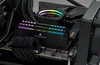
Corsair, G.Skill, and Kingston showcase their DDR5 RAM kits
3
Corsair, G.Skill, and Kingston showcase their DDR5 RAM kits
G.Skill boasts of DDR5-6800 RAM. Rivals aim at mainstream with DDR5-4800, 5200 kits.
 0
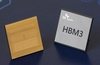
SK hynix boasts of its "industry first" HBM3 development
0
SK hynix boasts of its "industry first" HBM3 development
It claims that this TSV technology enhanced memory is "the fastest DRAM in the world".
 2
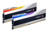
G.Skill Trident Z (RGB) 32GB memory kits announced
2
G.Skill Trident Z (RGB) 32GB memory kits announced
Samsung DDR5 IC packing 16GBx2 kits will launch at up to DDR5 6400 CL 36 speeds.


