


Production lines ahoy
The whole process operates in production line fashion, teams of robots and women placing the components on the mainboard in preparation for the solder process to attach them electrically and physically.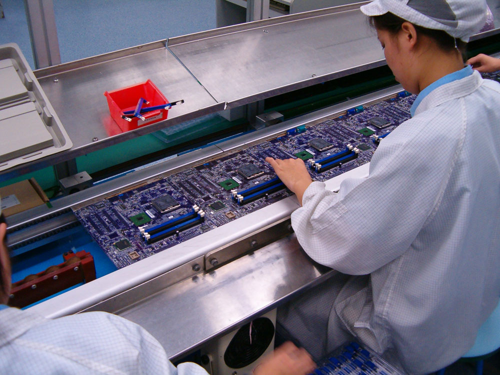
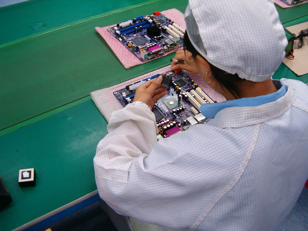
The photograph above shows part of the human element with memory slots being placed onto the ECS i915GL mainboards that Building 26 was currently producing on that floor. When all the components are in place, dropped on by female or robotic hand, the boards are fed in one-by-one to giant soldering machines, which solder the underside of the mainboard, attaching solder to the solder pads on the rear where the components lie. Since you're basically dipping the underneath of the mainboard into a solder bath, the height that the runners carry the mainboard over the solder is absolutely key to getting it right. ECS's soldering hardware is state of the art, able to vary the board height constantly during its journey through the machine, to micron precision, to make sure it's correct.
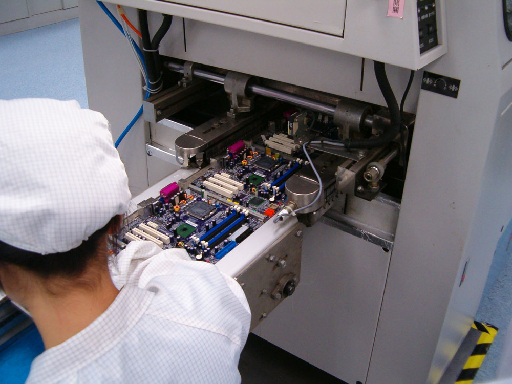
There you can see very nearly finished mainboards making their way out of one of the printing robots. Once done, they're passed through the solder machine, which cools them on the way out, like so.
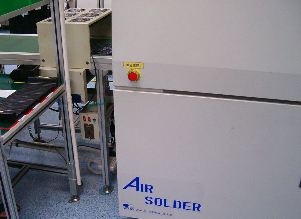
Notice the board passing under the fan array, to get it back down to a human-touchable temperature for visual inspection, and then final fixtures and fittings.

The shot above shows one of the visual inspection stages that are carried out every step of the way during production. The lady covers the mainboard with a plastic mask which shows the key components that she needs to check are in place and the right way round (if needed). Checking takes less than 30 seconds when the ladies are up to full speed. They follow their own pattern and procedure for the check, and were completely unfased by the horde of hacks and ECS staff that stood around pointing and chatting about the production process, literally right next to their stations.
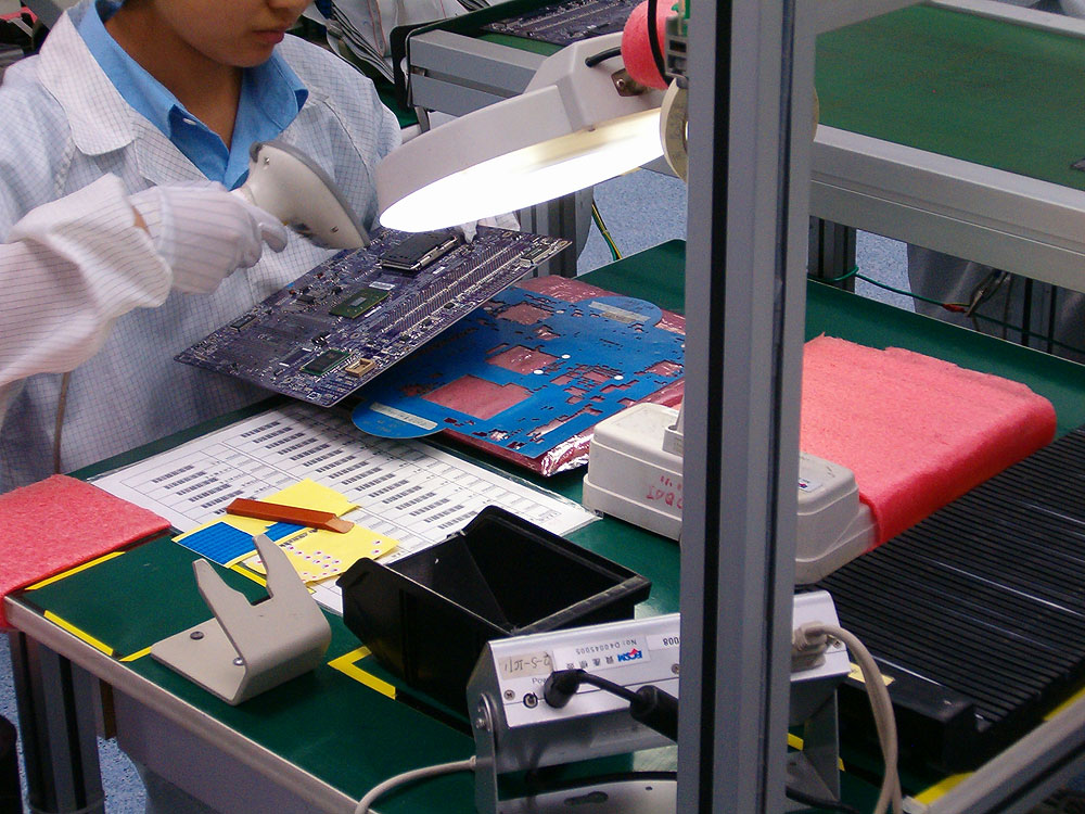
If it passes, she scans the barcode which updates a computer system with information about the check and just where in the production line that board is. ECS can track board production times down to the second, monitoring how long each step of the process takes. If someone is a bit slow at their station, the computer system will say so, and they can be encouraged to go a bit faster after their next break. Also, if a set of boards starts to fail the testing process, they can tell exactly which one of the many production lines in Building 26 was responsible and if needed, track down the exact employee that was responsible for the section of the mainboard that's failing the test.
Pretty much all that's left when the mainboard has been soldered is the heatsink placement and final board testing. The final production testing is done by skilled female technicians who have the ability to test two at a time, in tandem. They've got some test hardware that I'm jealous of (fast-removal memory modules, CPU heatsinks that don't need full attachment, PCI and PCI Express logic testers, etc.) and can have a mainboard fully functionally tested in a matter of minutes.

When that's done, a small sample of some 3% (Sigma Six sample confidence, I think) are sent to burn-in testing for 24 hours. If the batch passes burn-in testing, the entire batch run are packed up in their correct boxes and sent off to the distributors, ready for sale. At that point, that's the entire production lifecycle for the mainboard, from PCB production at Biloda to final testing and packing at Building 26 complete. The board then enters your hands after sale. Scarily, a board can make it from PCB production at Biloda to fully tested and packed at one of ECSM's buildings in under two days, start to finish. Board production in Building 26 takes only a few hours at most, from bare PCB to finished and functionally tested, with the longest part of the process the wait for the ~3% sample testing to pass burn-in.
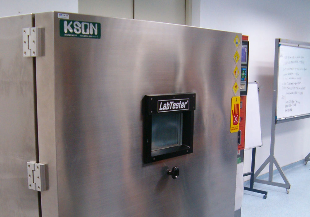
ECS also have some environment testing machines, where they can test mainboards in high-temperature, high-humidity conditions. Machines like this. Now if only HEXUS could get one of them into my office, I'd be able to say with extreme authority that the latest CPU has a bit of trouble running at 200°C ambient at 100% humidity


