


First you start with the PCB
The Biloda Factory
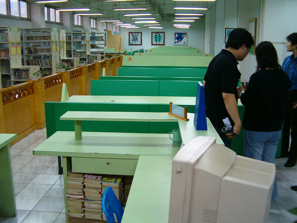
ECS's Biloda PCB factory is located less than an hour out of Hong Kong, on the outskirts of the city of ShenZhen, by car. The factory has a near 2000 resident workforce that live on-site in dormitory blocks located near to the factory. Workers have nothing more than a short walk to the factory gates to start their shift, with ECS providing everything you need to live and work in pretty much the same place. ECS make a big deal about keeping the resident workforce happy, with on-site restaurant and relaxation area, well kept garden for spending free time in, employee-built library that's entirely staff-less and run by a check-in/check-out computer system that somewhat mirrors the production tracking system ECS use on the factory floor. So while work and play are rarely separated, since it's a fair run in to ShenZhen city and you live directly on-site next to the factories, it's as pleasant as possible from what we saw.The factories are in production 24 hours a day, 7 days a week, run by the factory managers in a three-shift system. Entering the premises at Biloda is nothing more than finding somewhere to park, waving at security and walking in. We were warmly invited in to meet the factory's VP, Albert Lu, to receive a quick presentation on ECS, the PCB factory and why the company believes itself to be a very important part of the process, if not the most important, of making mainboards for PC products. Fully ISO certified and operating to stringent quality controls, which were backed up by observing the factory areas we were shown, Biloda is where the heart of many PCs are made.
Cutting, preparation and lamination are the first steps
So how does Biloda make a PCB? First it starts with the cutting and preparing of materials needed to make the PCB, be they metal layers, substrate layers, plastics used during lamination or anything else needed, to the right size. Industrial machinery takes the raw materials that Biloda sources and chops it up into the correct sizes, ready for feeding the laminating machines.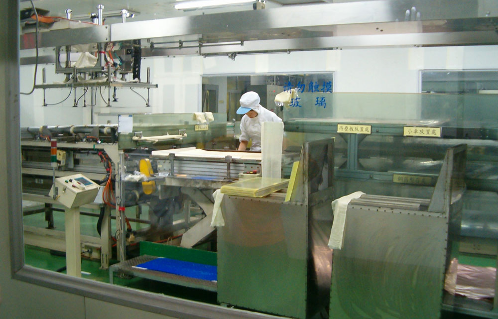
The machines in that picture above laminate the PCB substrate with a metal layer, producing a single layer on the mainboard, ready for pressing with others to create the full PCB assembly. Think of it as creating a giant material sandwich, adding layers as needed for the electrical requirements of the product you're creating. There's no need for an 8-layer PCB for a low-cost mainboard, since each layer adds a financial cost to the product, but for something like a mobile phone where the product, and therefore PCB, is small, something like a 12-layer PCB might be needed due to component density and the need to route traces in a small space. It all depends on the product you're creating.
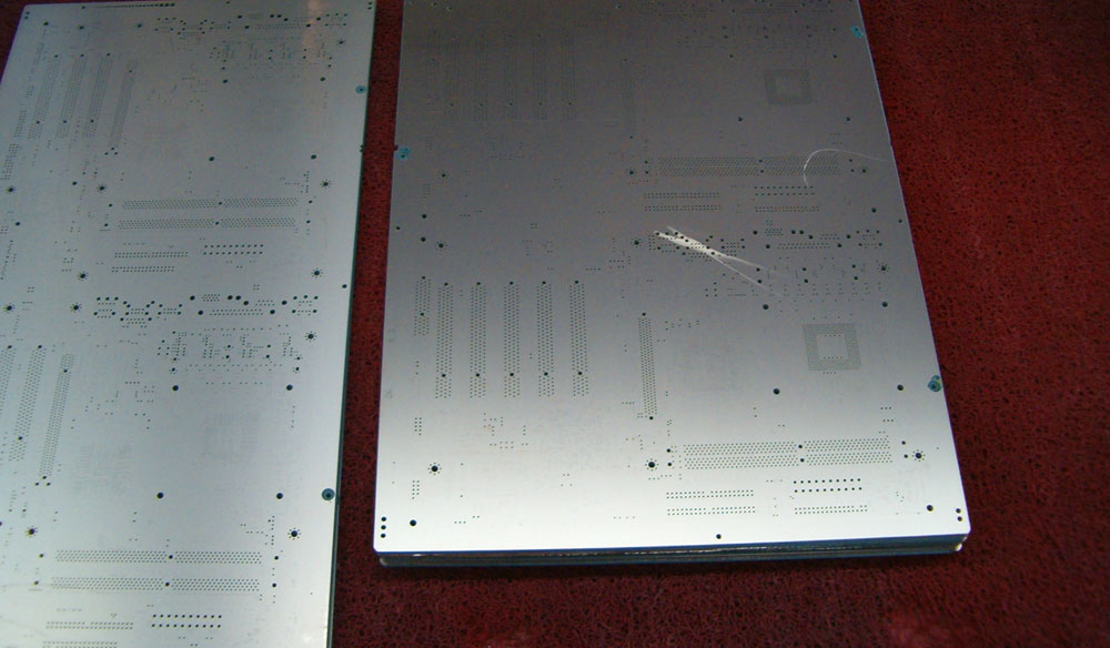
Next you drill the holes
Once you've pressed the layers to create the basic PCB with the requisite number of layers, you'll need to drill the holes required for the components the mainboard will hold. With a modern PC mainboard having over 3000 holes for all the components, there's no chance of doing this step by hand since the spacial accuracy has to be extremely high. Instead, a drilling robot does the grunt work. PCBs are manually loaded into the drilling machines, where the individual drill bits have a life span of some 1000 applications before needing sharpened, by hand. Skilled workers are needed here to make sure that this first major step of PCB assembly goes correctly. Line the basic pressed PCB up even a millimetre out and you ruin that board for the rest of production. Over 100 drilling machines, each with 6 robots, can be found at Biloda.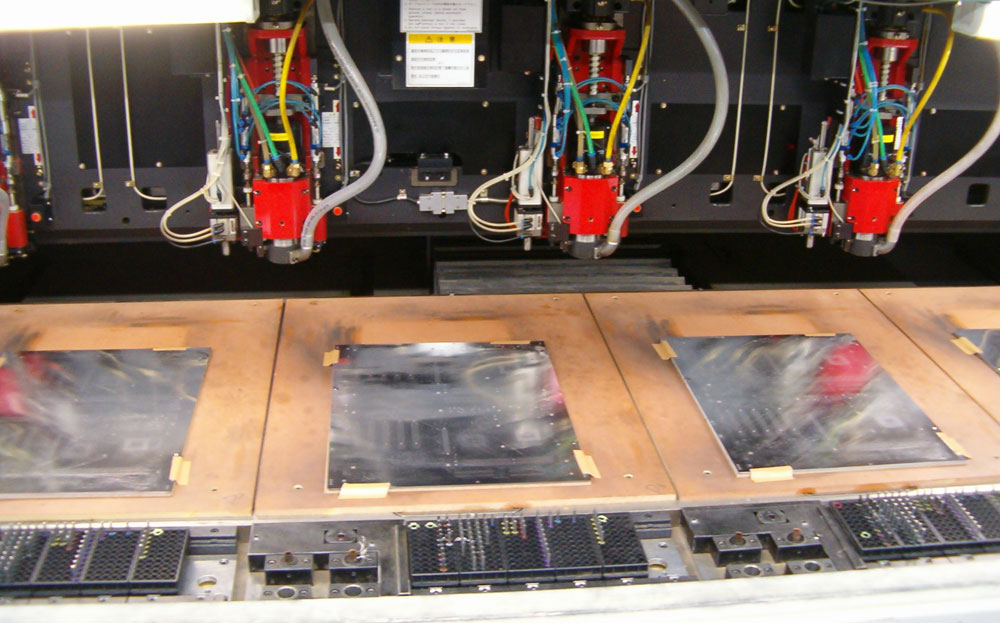
The robotic arms are programmed with the hole mask for the mainboard model being produced, to make sure it drills the holes in the correct places. The robot then proceeds to drill the holes through the basic PCB at high speed. Each robotic arm is only responsible for a certain section of the PCB and won't drill an entire design out on its own. Once it's finished its own section, the board is then loaded into the next machine ready for the next section to be drilled out. Final drilled boards can be seen here.
Exposure to UV to create the solder mask
Drilled boards are then sent for exposure to create the solder mask. ECS use UVE-5K C-Sun exposure machines to remove the material needed to create a successful solder mask.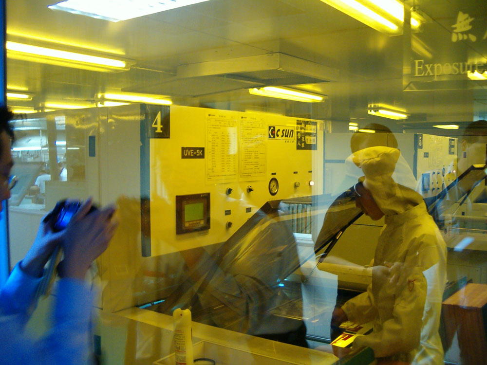
The UV exposure exposes the solder pads that solder will attach to, after component placement. Exposure using the 5kW lamps in the UVE-5K takes little time, allowing the PCB to proceed to the next part of the process, one that's arguably the most important.
Visual inspection every step of the way
A PCB doesn't pass through Biloda without hundreds of pairs of eyes watching it every step of the way. Once the UV exposure process is complete, the PCBs are sent to a room where a small army of women visually inspect the PCBs for defects that may have snuck in, usually during the drilling process. When a drill bit comes to the end of its usefulness as it becomes blunt, there's a small chance that a few of the final holes it'll be asked to make before sharpening happens again won't be complete. Visual inspection is designed to pick those up and if there's only one or two holes that haven't made it all the way through, they can maybe be done manually in a small workshop, to save the PCB being wasted.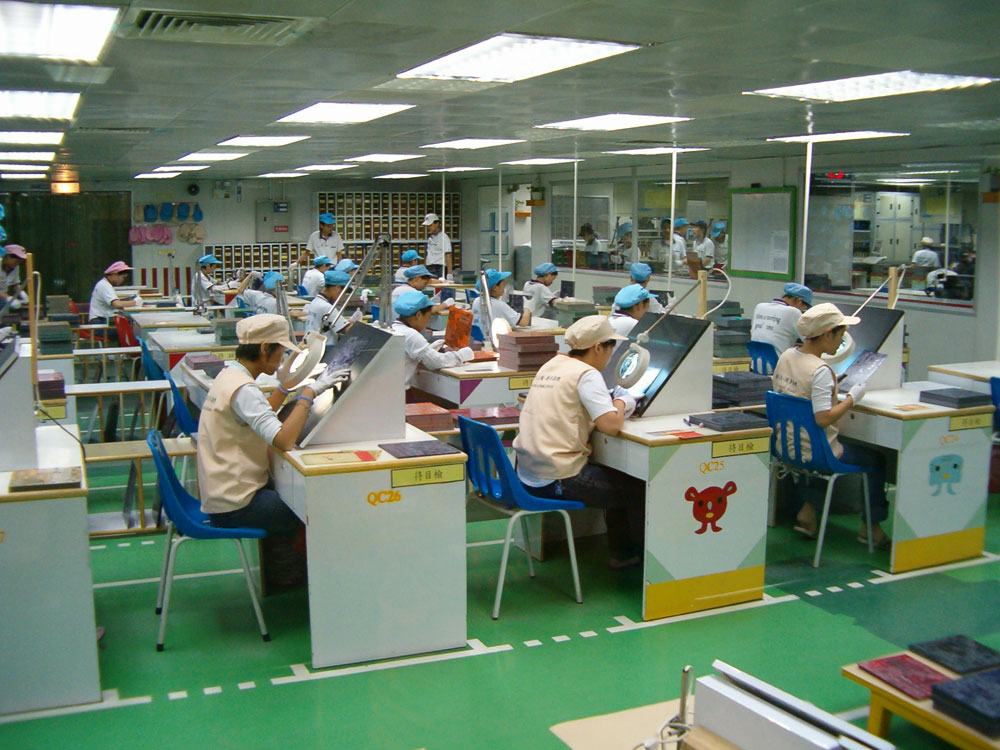
Screen printing so you can see what goes where
The next step is to screen print the PCB. If you've ever noticed the white writing on a mainboard, that's what's applied by screen printing. It's a fairly old fashioned process, not unlike screen printing something like a T-shirt. The PCB is loaded underneath the screen that'll let the paint through, the screen is pressed down onto the PCB and a paint is manually pushed through the screen and onto the PCB.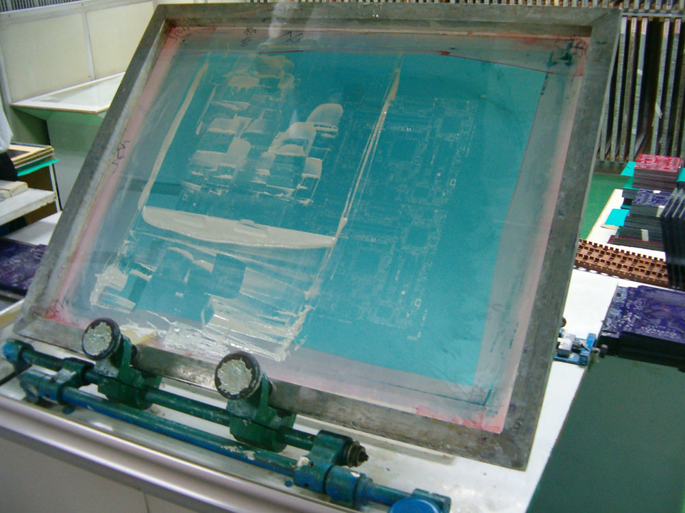
Looks like something in the art room at school, but can print something a bit finer than swear words on a T-shirt when the teacher wasn't looking!
Trimming round the edges and final testing
After screen printing, all that's needed to be done before the board can be sent out of Biloda to the customer is a quick trim round the PCB's edges to make sure it's smooth and free of defects, before visual inspection is done again and it's tested for electrical correctness on a test rig.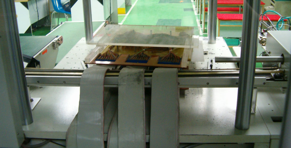
Underneath that top bit of machinery is a test mask that fits into every hole on the mainboard and tests the circuits inside for correctness. The ribbon cables coming out of the machine as you look at it are control ribbons for the computer program doing the testing. Boards are loaded manually but the electrical testing is all done by computer in Biloda. With nearly a thousand individual circuits to test, would you want to be the one doing it? It'd take hours manually whereas the robot can do it relatively quickly.
And with that, Biloda is done with the PCB, packing it and shipping it off to ECSM (or elsewhere) for the component application and solder dip that'll fix the parts and turn it into a working product.


