


Introduction
The last of the Fermis?Think of NVIDIA's Fermi architecture and the big beastie that's the GeForce GTX 480 springs to mind. The range-topping GPU is only one of six current Fermi-derived desktop products available, as the range has been fleshed out with the GTX 470, GTX 465, GTX 460, GTS 450 and, rather quietly, the OEM-only GT 420.
Common sense informs the savvy reader that NVIDIA hasn't quite brought Fermi to bear for all price points, then. There exists a rather large gap between the OEM GT 420 and partner-produced GTS 450. This is now filled by the DX11-compliant GeForce GT 430. Let us explain how NVIDIA got to it by trotting out the GTS 450's block diagram.
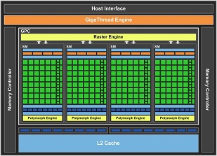
GTS 450 (as shipping)
This
is the high-level design of a shipping GTS 450. It constitutes a
cut-down version of the full GF 106 architecture (GeForce GTX 460).
Made up of four
Streaming Multiprocessor units that are home to 48 shader processors
and eight texture-units each, the card-wide tally is 192 SPs and 32
TUs. These are backed up by a total of 16 ROPs that are connected to
two 64-bit memory buses and through to external GDDR5 memory. Keeping
the
GPU
ticking along is 256KB of L2 cache. OK with that number overload?
Chop suey
With the aim of making Fermi cheaper for the GT 430 part, NVIDIA cuts right down the processing heart of the GPU and removes two of the SM units and, relatedly, 16 texture units - basically halving the computational power of the chip. One would expect a commensurate reduction in the memory bandwidth with a 64-bit partition deactivated, but NVIDIA keeps the 128-bit bus backend of the GTS 450 intact in the move to the new GPU. The ROPs though get a chop from 16 to four.
Do the math and you'll determine that the GT 430 has 96 shader processors, 16 texturing units and four ROPs that are connected to a 128-bit memory bus. The GPU's supplemented by 128KB of L2 cache, as well.
Making some comparative sense of it all, here it is stacked up against the GTS 450, AMD Radeon HD 5550 (GDDR3), HD 5670 and HD 5750 GPUs.
| Graphics cards | NVIDIA GeForce GT 430 1,024MB | NVIDIA GeForce GTS 450 1,024MB | AMD Radeon HD 5550 1,024MB | ATI Radeon HD 5670 1,024MB | ATI Radeon HD 5750 1,024MB |
|---|---|---|---|---|---|
| Die size | 0.58bn | 1.17bn | 0.63bn | 0.63bn | 1.04bn |
| Manufacturing process | TSMC, 40nm | TSMC, 40nm | TSMC, 40nm | TSMC, 40nm | TSMC, 40nm |
| General clock | 700MHz | 783MHz | 550MHz | 775MHz | 700MHz |
| Shader clock | 1,400MHz | 1,566MHz | 550MHz | 775MHz | 700MHz |
| Memory clock (effective) | 1,800MHz | 3,608MHz | 1,800MHz | 4,000MHz | 4,600MHz |
| Memory interface and size | 128-bit, 1,024MB, GDDR3 | 128-bit, 1,024MB, GDDR5 | 128-bit,
1,024MB, GDDR5 |
128-bit,
1,024MB, GDDR5 |
128-bit,
1,024MB, GDDR5 |
| Memory bandwidth | 28.8GB/s |
57.7GB/s |
28.8GB/s |
64GB/s | 73.6GB/s |
| DirectX/ Shader Model | DX11, 5.0 | DX11, 5.0 | DX11, 5.0 | DX11, 5.0 | DX11, 5.0 |
| Shaders | 96 | 192 | 320 | 400 | 720 |
| Single-precision GFLOPS | 268.8 |
601.3 |
352 |
620 |
1,008 |
| Texturing | 16ppc
bilinear 8ppc FP16 |
32ppc
bilinear 16ppc FP16 |
16ppc
bilinear 8ppc FP16 |
20ppc
bilinear 10ppc FP16 |
36ppc
bilinear 18ppc FP16 |
| ROPs | 4 |
16 |
8 | 8 |
16 |
| GPixels/s throughput | 2.8 |
12.5 |
4.4 |
6.2 | 11.2 |
| GTexel/s bilinear | 11.2 |
25.1 |
8.8 |
15.5 |
25.2 |
| Multi-GPU | No | Two-way SLI | Two-way XFire | Four-way XFire | Four-way XFire |
| Connectors (native) | Dual-link DVI HDMI VGA |
2x
dual-link DVI Mini-HDMI |
2x
dual-link DVI HDMI, DisplayPort |
2x
dual-link DVI HDMI, DisplayPort, |
2x
dual-link DVI HDMI, DisplayPort, |
| TDP (max) | 49W |
106W |
39W | 64W |
86W |
| Retail price | £60
($79) |
£99
($129) |
£60 ($79) | £80 ($115) | £90 ($125) |
Analysis
The decision to keep a 128-bit memory bus pays dividends for NVIDIA, because it means that slower-speed, cheaper graphics memory can be used without really hampering the card's bandwidth.
We suspect pricing is going to be closest to the Radeon HD 5550 GDDR3 and, on paper, the Radeon has the beating of the GeForce - comfortably so going by the specs.
It's not a gaming card per se, says NVIDIA
But these low-end cards aren't really about gaming prowess. Rather, they're upgrades over integrated graphics and serve as general purpose GPUs that are adept at handling multimedia tasks and HTPC apps. Both NVIDIA and AMD support audio bitstreaming of DTS-HD and Dolby TrueHD over HDMI (read Blu-ray playback). Reinforcing the non-gaming bias of the GPU is the lack of multi-GPU SLI compatibility.
Going by the numbers, the cheapest Fermi card that you can put your mitts on seems to provide a decent mix of specifications, features and price. NVIDIA wants you to think of it as a core component of a modern 'digital' PC- a good fit for a multitude of different types of computer - and there's some merit in this line of thought.
Pragmatism
The majority of GT 430 cards will be shipped to system builders for integration into fully-built-up PCs, according to NVIDIA. Partners will be given carte blanche at designing their own PCBs and cooling solutions, so expect to see passive models, half-height cards, and some weird and wonderful mini-heatsinks.
Segueing nicely, we take a look at an ASUS GeForce GT 430. Keep on readin'.


