


Introduction and architecture analysis
NVIDIA launched its latest graphics-card architecture at the end of March this year. Built on a DX11 design known as GF100, two high-end cards, GeForce GTX 480 and GTX 470, were available a short time after launch, and a third, GeForce GTX 465, was released in late May.Manufactured using a large chip with some three billion transistors, GF100-based cards are inherently expensive. GTX 465 pops up for £210, GTX 470 weighs in at £260, and the top-line GTX 480 for a not inconsiderable £375.
NVIDIA's next move, predictably enough, is to take much of the goodness in the GF100 architecture and reduce it down such that retailers are able to hit sub-£200 price points. Now some three months after initial launch, NVIDIA is ready to tackle the mainstream market with the GF104-based GeForce GTX 460, which is to be made available in two configurations.
GF100 vs. GF104
NVIDIA has chosen to use a slightly different architecture and GPU layout for the mid-range Fermi parts. Rather than turn the off-switch on portions of the GF100 GPU - which, remember, is very expensive to produce, being based on silicon that's 529mm² - the company is using the latest manufacturing know-how and opting for a smaller GPU, known as GF104, to provide the backbone for both versions of the GeForce GTX 460.
To understand how the premium GF100 and the new GF104 GPUs differ, it is necessary to whip out the ever-so-useful block diagram.
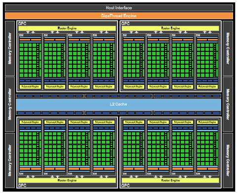
GF100 - 512-core version
In its optimum form, GF100 is composed of four GPC (Graphics Processing Clusters) that are in turn made up of four SM (Streaming Multiprocessors) which are home to 32 CUDA cores each. Do the math and this leads to a GPU-wide tally of 512 cores. Putting pragmatism ahead of theory, even NVIDIA's GeForce GTX 480 isn't a complete GF100 part, because, in the interests of economics and yields, it has one SM switched off, leading to 480 cores over 15 SMs.
Drilling down, each SM features four texture-units and what NVIDIA terms a 'PolyMorph Engine.' The purpose of this engine is to boost geometry processing through tessellation - a DX11 feature that NVIDIA sees as a key driver for better-looking games. GF104 keeps to the same basic GPU philosophy but shuffles the SM arrangement with the view of creating a smaller die - 1.95bn transistors rather than the 3.0bn on GF100-based cards such as GTX 465, 470, and 480.
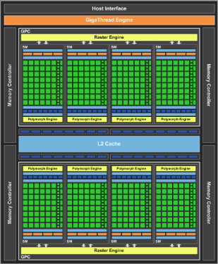
GF104 - full-fat version
NVIDIA's focus is to cram as much Fermi power into a smaller die, clearly. Rather than simply cleave the GF100 design into two, leading to 256 cores, which we reckon is too low to be competitive with ATI's Radeon HD 5800-series cards, NVIDIA trims the design to use two GPCs and eight SMs. The logical assumption would be that it is half a GF100 but the devil is in the details.
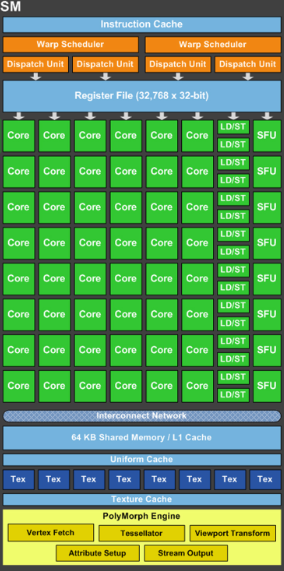
GF104 SM
NVIDIA has bolstered each SM with more cores - 48 vs. 32 in GF100 - notice how the green squares are more numerous in GF104? The increase in per-SM cores is augmented by a doubling of the texture-units, from four to eight. Looking at the top, decoupled from the SM itself, there's a doubling of dispatch units and, lower down, special-function units when compared to GF100. These are needed to service the extra CUDA cores per block.
Much like GTX 480, NVIDIA leaves some wiggle room with GTX 460
The GF104 layout shows that GTX 460 is optimally composed of eight SMs, amounting to some 384 CUDA cores (48 x 8). In the interests of protecting the GF100 cards from mid-range GF104 attack and with a nod to the vagaries of silicon production and yields, NVIDIA deactivates one SM on the GTX 460s. We may well see it activated in the future as yields improved, however.
Equipped with seven SMs, then, the mid-range GeForce GTX 460 has 336 cores, just shy of the GeForce GTX 465's 352. However, the doubling of texturing capability means that the new GPU possesses 56 texture-units, compared to 44 for GTX 465. On the downside, there are now fewer PolyMorph and raster engines to handle all that tessellation. It's a give-and-take setup when judged next to the cheapest GF100 card.
GeForce GTX 460 in two flavours
GeForce GTX 460 ships with a 1,024MB framebuffer connected to a 256-bit-wide memory-bus and to 32 raster back-ends (ROPs) just like GeForce GTX 465. Commonality extends to having 512KB of L2 cache supporting GPU operations across GPCs.
A second, cheaper version of GTX 460 is also launching at the same time. Endowed with the same 336 cores made possible by using the same seven SMs, it provides 768MB of GDDR5 memory through a narrower 192-bit bus, together with 24 ROPs and 384KB of L2 cache. The reason for having a second GTX 460 lies with hitting the very desirable $199 price point.
The architecture examination hints that the GeForce GTX 460 1,024MB will perform similarly to a GTX 465, losing a bit of geometry performance but clawing it back in shading and texturing. Of course, any performance predictions are useless without a knowledge of clock-speeds, so let's head on over to a handy table.


