


Architecture musings I
There, I've said it.
I'm going to say it right at the top of this page so that it's inescapable - AMD's much-vaunted R600 isn't as fast as NVIDIA's GeForce 8800 GTX, never mind the recently-reviewed GeForce 8800 Ultra SKU. You'll see why as we take a look at the architecture.AMD realised that it can't compete on performance alone and has had to take the unenviable step of introducing its top-of-the-line DX10 graphics card at just $399. That's around £250, or GeForce 8800 GTS 640 money. So, please do bear in mind the value-for-money aspect when considering the technology and performance.

DX10 changing the face of shading: R600's unified shading architecture
Until now, all ATI desktop graphics processing units (notice that I'm purposely ignoring the Xenos GPU inside the Xbox 360) have been designed to work on geometry data (vertices) passed on by the host CPU in a system, through discrete vertex shaders which transform and lights them. These transformed vertices (grouped into triangles), which are the building blocks of any scene, are then passed on to separate pixel shaders for processing of the individual pixels of the triangle(s), making them look realistic via the use of texturing, bump mapping and so forth.Now, the introduction of DX10 requires that the traditional pass-through of vertex to pixel shading be modified such that 'general stream processing units' can work on either, depending entirely upon load. That's important to note because, previously, GPU designers have had to take a best-guess at vertex-to-pixel shading ratios: some scenes may require only a little vertex shading and place a large emphasis on turning the pixels into pretty pictures, others may require the opposite. GPU shading utilisation, then, was problematic before DX10 laid down the unified spec. With a USA there's no more '8' vertex shaders and '36' pixel shaders; it's all one and the same now, depending upon how the threads are scheduled.
Looking at the block diagram of the Radeon HD 2900 XT and taking into account the need for a unified shading architecture, we see that the mid-section is where the stream processing goes about it business, working on various kinds of data. More on these in a moment.
Setting it all up
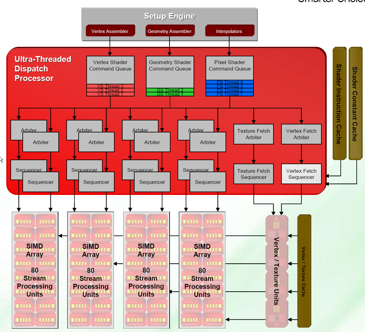
Much like NVIDIA's GeForce 8800 - and kind of mandated by adhering to DX10 spec - AMD's R600 uses an intelligent setup engine to prepare data to be fed to multi-purpose stream processors. For R600, the stream processors are bunched in groups of four and each is defined as a Single Instruction Multiple Data (SIMD) array that works on data in parallel. The point of the setup engine is to keep the stream processors as busy as possible.
Each SIMD array has a couple of arbiter units that schedule work (normally threads) to that array and it alone - a new thread gets dispatched to the ALU monster every other clock- cycle. The sequencers, sitting just below, help determine the size of the thread (shaders can be long, long beasties) and ensure that threads are suspended/restarted as needs be.
The dispatch processor, then, keeps track of hundreds of threads to keep the SIMD arrays - and, say, texture fetching - busy, thereby keeping that nasty word in GPU design, latency, down to a minimum via the use of massive parallelism. Threads are evaluated in terms of time to execution and, carrying on the dynamics further, any thread can be suspended should it stall the pipeline. It's all about efficiency when you have 320 stream processors and a bunch of texturing units waiting for instructions and the back-end waiting for bandwidth.
Looking to the right, R600 uses virtualised, associative caches to load huge instruction sets (shaders) from system or local memory which are then executed as the dispatcher sees fit.
Going up a step, you'll also note the presence of a geometry assembler, for the geometry shader (another DX10 mandate) that lies between the vertex and pixel shaders and can massively increase the vertex ability of the GPU by using the data present after the vertex shader has done its work and add to it by creating new triangles. Further, it can work on multiple vertices concurrently, something that a vertex shader cannot do. Think of it as vertex shading beefed up, creating more geometry and helping the CPU out.
Tesselate me, baby
What's that stuck on to the end of the vertex assembler? A programmable tessellator, that's what.Also present in the Xbox 360, think of a programmable tesselator as a geometry shader on steroids. Game developers would love to use high-polygon models for all assets in a game - everything will look good, naturally. The main problem in dealing with models consisting of millions of triangles is one of storage - they swamp the vertex buffer quickly.
To achieve the same effect in an efficient manner, the entire HD 2000 series uses a programmable triangle tesselator that takes a low-res triangle mesh and subdivides it (for a greater number of triangles) to generate greater mesh detail. AMD highlighted an example of hardware tessellation that took a 1,000 polygon model and tessellated it to 430,000 polygons, via a variety of higher-order surfaces.
The idea is to replicate a high-polygon model with an initial coarse model with a small memory-footprint. That's why the tesselator sits directly above the vertex shader, feeding in its amplified output that the CPU didn't have to generate. We should see it make an obligatory appearance in DX11. All good so far.
Stream processing
Coming to the large chunk of processing units in the middle and thinking about the unified nature of the R600, where any stream processor can work on any kind of data, AMD packs in a total of 64 (16 x 4 SIMD) processors that comprise of a five-way superscalar ALU setup. Let's explain that a little further and think about pure processing ability.
Previous iterations of ATI hardware used a vector-based approach to processing. R5xx used vec4+1 and AMD's sought to keep the structure the same but made each ALU independent in terms of execution.
Putting it another way, AMD's followed NVIDIA's lead and understood that breaking down processing into pure scalar units is better for compute flexibility and efficiency than, say, having a vector-based setup where, for want of a better word, you may be 'wasting' resources by apportioning a chunk of processing where numerous scalar units will do the job with better granularity.
The fatter processor in each block also handles what are termed transcendental instructions (the likes of SIN, COS, LOG, etc.). DX10 also does away with partial precision and demands 32-bit (128-bit for RGBA) floating-point precision - and AMD adheres to it.
There's also a branch-execution unit that's used as a kind of control logic that arbitrates (word of the day) when and how parts of shader code can be 'branched' (skip, write, for example).
This per-stream unit takes away the need for the ALUs to do it. Further, the ALUs hook up to general purpose registers that store temporary data required for computation. Think of it as a home to thread data while it travels down its merry way.
In total, then, Radeon HD 2900 XT packs in 320 (64x5) processing units that can issue Multiply-Add (MUL + ADD = MADD) instructions per clock. That compares favourably with NVIDIA's 128 SPs for its GTX/Ultra cards but the devil is in the details.
AMD doesn't use different clock domains for its HD 2000-series cards. Rather, in the case of the HD 2900 XT, the shading core is clocked in at 742MHz, and with 320 processors operating on two instructions per clock, it adds up to a 475GigaFLOPs. NVIDIA's GeForce 8800 Ultra's shaders operate at 1.5GHz and process three per clock, giving a theoretical 576GigaFLOPs, although there's always the question of that missing MUL.


