


Reference Board Examination
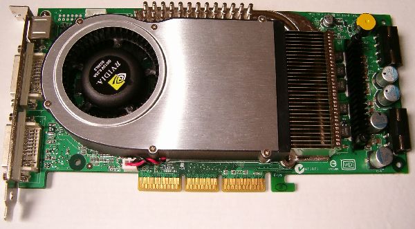
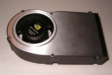
The board might be a surprise to some. For those expecting the cooler seen in some shots leaked from press data, that cooler is for the non-Ultra version, with the Ultra sporting an obviously different reference cooler. It's a modified version of the cooler used on the 5950 Ultra reference board, using the same rotary blower to move air over the GPU heatsink.
It's a 1.5 slot cooler, taking up only one slot on the ATX backplane, but encroaching on the first PCI slot in terms of heatsink assembly height. You can still put something on the PCI backplane space, but nothing in the slot. How useful that is depends largely on any motherboard bundle you have.
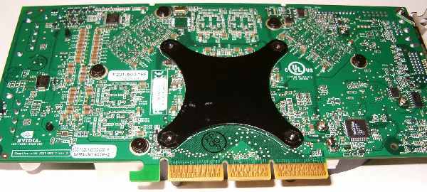
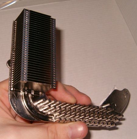
The heatsink assembly itself is a four part affair, if you include the retention bracket on the board reverse.
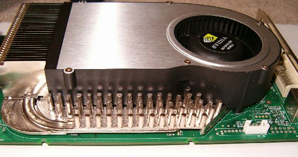
The three silver Philips screws on the right hand side of the PCB, as you can see it in that picture, let the DC blower and its shroud free from the board. Unclipping the fan plug is simple. That leaves you with this.
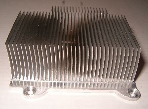
The memory heatsink is one piece, the GPU heatsink another. Both are aluminium, the GPU cooler especially lightweight and rather flimsy in its fin construction. More on temperatures later.
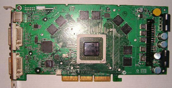
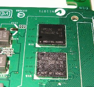
Getting the memory heatsink off is simple, just unscrew five spring loaded black screws from the board reverse. The DRAMs (Samsung's K4J55323QF GC-16 parts) are GDDR3, 600MHz rated, and interface with the heatsink via thermal pads.
8 256Mbit DRAMs in total, arranged around the top and right of the GPU. There are no DRAMs on the back of the board, 8 256Mbit chips giving the full complement of 256MB.
The GPU heatsink is removed by means of four silver spring loaded screws from the top side of the sink. That reveals the GPU (after cleaning the die of its supplied thermal interface material).
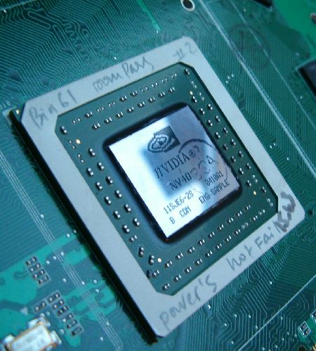
There are definitely some things worth talking about here. The die is massive, etched with the GPU codename, a little NVIDIA logo bitmap and some miscellaneous GPU information. It's A1 silicon, both the die etching and the driver report the same information. Using different packaging from recent NV3x GPUs, the die is bare.
Also worth noting are the pencil inscriptions on the raised shim around the core area, on top of the packaging. The review samples are hand tested for correct operation. Making a guess at what the writing means, the GPU I tested came from bin 61 and was the second die to pass testing. The bottom edge of the shim says either "power's hot fail" or "power's not fail", I'm not sure. I'm guessing the latter, since it was released for reviewing. I've no idea what "15.63" means.
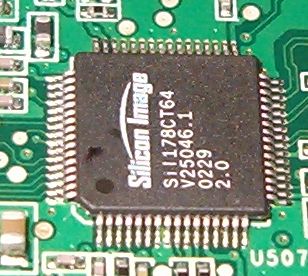
Dual DVI makes its first appearance on a reference consumer accelerator from NVIDIA. The DVI operation on the reference board was flawed, something that should be remedied by retail release. I'll outline the problem encountered later. Silicon Image get TMDS #2 duties on the reference board, their Sil178CT64 ASIC running the second DVI port.
Completely assembled, the entire graphics card and heatsink assembly weighs 396g. A quick comparison with the other cards I have access to puts it lighter than ASUS' Radeon 9800XT (458g) but heavier than Point of View's GeForce FX 5900XT (332g) and NVIDIA's GDDR3 5700 Ultra reference board (350g).
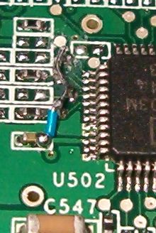
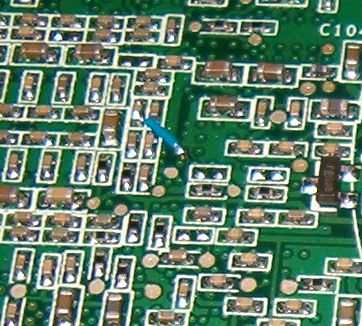
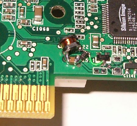
The reference board also contains a number of post production modifications to ensure it works correctly. Two wires and a small copper coil have been added to the board after creation. That might not be the case with other reviewer's samples and definitely won't be the case at retail, but it's worth bearing in mind.
The capacitors appear to be 1500µF, 16V caps, but I can't be certain, their inscriptions aren't helpful in tracking down the specific parts. Two Molex connectors provide power to the board. NVIDIA recommends a 480W power supply and you have to power each Molex using separate lines from the PSU, not using a Y-splitter. I'll cover the power requirements a bit later.


