


Packaging it all up
Back in November 2017, Intel released high-level details of a bold, new play for the gaming notebook market, identified as a high-growth area for 2018.
The news centred on a partnership between Intel and AMD, where the latter would supply its graphics know-how and enable Intel to build a single chip containing its own class-leading CPU cores, AMD graphics, and HBM2 memory.
The purpose of such a chip is to provide a robust gaming experience in a thinner laptop profile and with less power than if going down the Intel CPU and discrete AMD/Nvidia GPU route alone. And there's a fair chance that any products equipped with this new processor will be cheaper, too.
To be clear, though partnership in name, any resulting products from this collaboration belong entirely to Intel, because AMD is taking the same semi-custom technology position that it has successfully done so with the console guys.
Today, Intel is ready to put more meat on this intriguing product's bones, so let's see just what is under the hood.
EMIB to to the fore
Intel is debuting this fusion of technology by releasing five Core processors. The chips are based on the presently-available, performance Core H-series chips found on most high-end laptops, and this means they use a quad-core Kaby Lake CPU architecture that's great for single-threaded applications and solid for multi-threaded apps.
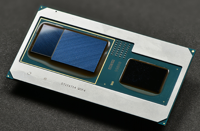
That chip is shown on the right-hand side (ignore the H-series typo) of package graphic and it hooks up to the Radeon GPU via a standard PCIe Gen 3 x8 interface, just as it would likely do if the Radeon GPU was a discrete card.
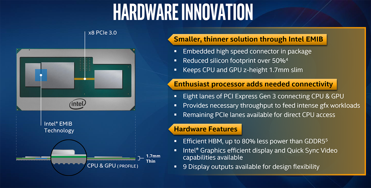
The real innovation from Intel's side is having the ability of connecting a custom GPU to HBM2 memory at high speeds and low latency. The connecting technology is called EMIB (Embedded Multi-die Interconnect Bridge), and it works much like a traditional silicon interposer but has the benefit of lower implementation cost and a lower z-height, which is important when building sleek gaming laptops.
The EMIB technology works by having multiple silicon bridges positioned inside the package substrate. Each bridge has four metal layers serving as interconnects and the way that the Intel Custom Foundry has built them means they have an interface pitch, at just 55 micrometres, which also happens to be the same interface used by HBM2 memory.
The benefits of this approach have positive ramifications for package size and power. Intel reckons this single-package solution cuts the traditional CPU+GPU+GDDR5 memory board real estate by over half, leaving gaming laptop makers an opportunity of either adding other ASICs or reducing the complexity of the overall PCB.
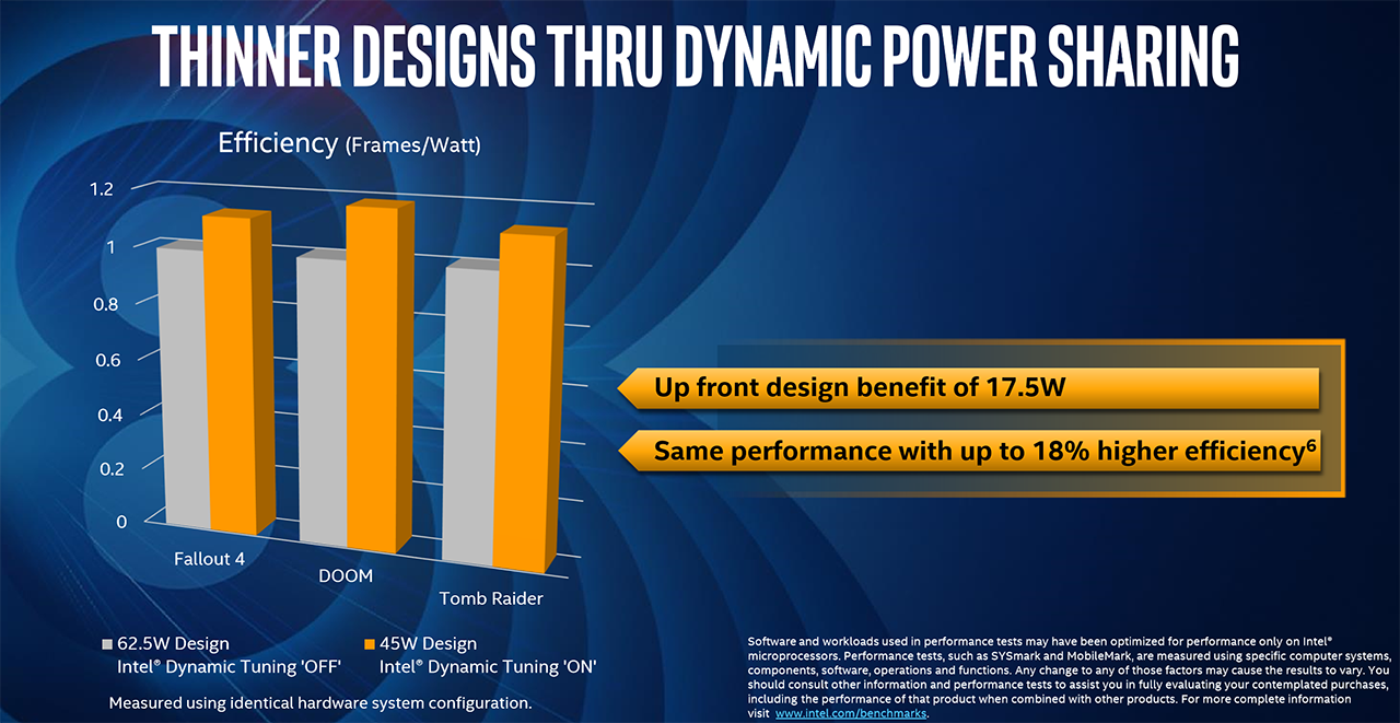
Arguably more important are power savings that result when moving from a number of discrete packages to a single chip. Intel explained that most gaming laptops are designed to a system design point, where neither the CPU nor the GPU are able to exceed in the interests of stability. Designing to a package TDP and using updated power policies, which Intel calls Dynamic Tuning, enables this one-chip solution to offer the same performance as an otherwise discrete setup but at a lower power cost.
Point is, as we have seen with AMD APUs, putting everything on one package means that SoC-level optimisations come into play. Intel cites being able to offer the same performance with 18 per cent less power, or, putting it another way, there is scope to increase the power and performance without increasing the system's TDP over traditional levels.


