|
NVIDIA have had a lot of criticism recently from various corners of the computing world. 5800 Ultra was too noisy, took up too many slots and wasn't appreciably faster than its direct competitor. Then the recent furore over their drivers and the application level optimisations they'd been performing on certain popular benchmarks. But look past the crap and you see a healthy company with a decent product line and a good comeback from recent issues, in this reviewers eyes at least.
The board I'm about to look at today is one such come back. The midrange sector is vitally important to any mainstream consumer graphics company. It's where they make the most money and it's the sector most likely to give them a surprise come the end of the quarter and sales are being totalled up, good or bad.
So recently, with their assault on the high end with FX5900 Ultra and a genuine competitor to ATI's recent high end monster boards, it's been time for them to also concentrate on getting the midrange right. High end success means brand awareness, midrange brings home the bacon. With ATI scaling performance back slightly in their midrange offering, with 9600 Pro being a little slower than its outgoing brethren, 9500 Pro, now is the time for NVIDIA to strike.
So recently we've seen the sneaky rollout of an uprated FX5600 Ultra part, the 9600 Pro's direct competitor. No flashy publicity, just a new set of cards shipped to the usual suspects for review and the same uprated parts sent to board partners who effectively get higher performance midrange NVIDIA offerings for free. The GPU will cost the same to partners and board prices using the new GPU will hopefully be static compared to older FX5600 Ultra's.
So what exactly are you getting with this new part, and why no new name like FX5700 Ultra? Here's a quick rundown of the GPU's features, comparing old to new.
| New FX5600 Ultra | Old FX5600 Ultra |
| Render pipelines |
4 |
4 |
| Texture units per pipeline |
1 |
1 |
| Shader units per pipeline |
1 |
1 |
| Core clock |
400MHz |
350MHz |
| Memory clock |
800MHz DDR |
700MHz DDR |
| Memory bus width |
128-bit/16-byte |
128-bit/16-byte |
| Memory bandwidth |
~12.8GB/sec |
~11.2GB/sec |
| Pixel fillrate |
1600Mpixels/sec |
1400Mpixels/sec |
| Texel fillrate |
1600Mtexels/sec |
1400Mtexels/sec |
|
So a rough 14.5% percent increase over the old model in all the key areas, memory bandwidth and pixel and texel fillrates. No change in architecture versus the older model, just increases in clock speed. It's still a regular GeForce FX GPU with all that brings to the table.
Let's take a look at the card itself before we move on to the test system and the benchmarks.
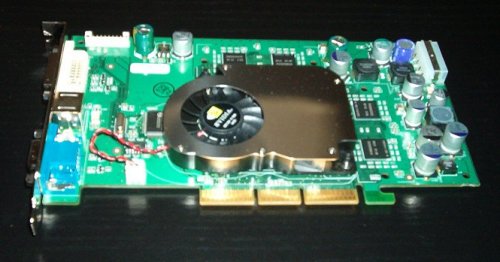 FX5600 Ultra Volume 2
The reference card sports a heatsink and fan assembly that is surely the shiniest in the industry. My absymal digital camera skills don't pick it out very well, but the front face on the heatsink is mirror like. In the right light you can double your PCI slots. We've got the usual 4 pin Molex style connector on the top right, and the board arrived with a Y-splitter just incase I couldn't find a spare connector from the quarter billion my Enermax PSU provides. Expect a nifty splitter in the retail box.
The Hynix 2.2ns memory chips are uncooled, relying only on ambient air flow to remove their heat. Not bad for modules running at 800MHz, however their 2.2ns rating does offer up the possibility of 900MHz operation, something we'll look at later. Memory density is 128MB, made up of 4 16MB chips on each side of the PCB. No fancy coloured PCB, just the usual snot green.
As far as connectors go, it's the usual. DVI-I, S-Video and regular VGA all make an appearance. Just like ATI's recent offerings, DVI and S-Video share an output.
A Philips SAA7114H TV processor is half hidden underneath the heatsink arrangement, but it's certainly present. Hopefully the majority of shipping FX5600 Ultra solutions will carry the processor for full TV output and capture, since the diminutive bit of silicon does both.
Lastly, there's some sort of simple I/O header present on the PCB, up near the top left as you look at that picture. Operation unknown.
System setup and benchmarks next.
|


