Intel P4 Review
Well we have seen a lot of articles and stuff
on the net about this CPU, with several different views. Hopefully this article
should cover all the main points out there.
AMD and Intel have finally decided to go their own ways in the form of CPUs.
Before we had AMD, the 'underdog', chasing Intel for the top spot, which some
people out there will finally believe that they have done. AMD ditched the
socket 7 interface just under 2 years ago now, and they haven’t looked back.
They went on to the Slot A interface (SECC1 format), and then on to the more
successful Socket A interface (which is there current format and will also be
the format for the Palomino...). The first Athlon (Gen 7) was the first "new"
CPU on the market.
The Pentium 4 CPU :-
Intel needed to kill this CPU quick, so they started new and clean. They had the
Pentium Pro, P2, P3, Xeon and Celeron 2 which were all the old "style" running
in the P6 architecture. To try and combat the market Intel added things like SSE
and MMX which were in competition to AMD's 3DNow technology. They also changed
the format of the interface from Slot 1 to Socket 370. The other changes they
have done are on DIE cache and other small changes, but they carried on working
on the same original template.
'So what?' I hear you cry. The P4 is setup around the new NETBurst architecture.
It is their attempt to finally knock AMD out. Intel were in a catch 22
situation. In the P3 vs. the Athlon war they were not performing too well due to
AMDs new more advanced design. The CPUs when under the same conditions clearly
showed that AMD's CPU was a winner. But Intel claimed that it wasn’t down to
this, it was just the P3 wasn't designed as a platform to run at this speed.
The big race was won by AMD when they hit the 1GHz first; and they do a
cheap-per-unit pricing strategy. AMD have carried on pushing their CPUs faster
and faster. They are now running at 1.33 gig which is soon to be updated to 1.4.
AMD developed a CPU which was happy at running at a high clock speed, or more so
than the Intel unit.
So why did Intel chose NETBurst?... Well NETBurst is the new development made by
the men in blue at Intel. The main catch is clock - to - clock performance. The
number of commands or instructions which can be performed by the CPU is low, but
they should be able to extend the platform and hit some high clock speeds. Intel
had to stick there heads above the parapets to do this design, but what did they
change?
Within the P3 they had a pipeline of 10 stages. Within the P4 it has been
doubled giving it more bandwidth. This is the main calculation and prediction
pipeline within the CPU. Having this with such high bandwidth will allow them
room to push the clock speed higher on the units. The pipe can be used more
therefore more instructions at higher speeds can be catered for. The way that
CPUS can be so fast is that they predict a lot of the outcomes before they need
to. This means that the system is ready but this can also cause a problem if the
system gets it wrong. So Intel had to improve the prediction unit within the
Core of the CPU. They say that they have cut this by around 35% over the older
P6 development. They also pushed dual ALUs into the system, which means that the
CPU is running "twice" as fast, like 1.4GHz running at 2.8. This means that the
CPU shouldn’t feel any latent affects of the deep pipeline.
They have added the SSE2 extension set to the CPU, which means that there are
144 new instructions, which will probably never be used but are useful to have
there anyway.
Intel decided to change the cache layout from the old-style crush-and-munch
cache which is used on the Athlon and the x86 architecture. The NETBurst setup
should auto-deal with these instructions within the execution trace. Intel have
also cut the size of the L1 cache size to 8K, yes this is 1/2 the size of the
P3. The idea is it will push the data through it quicker to fill the high
"bandwidth" pipeline. They run the bus at 100 MHz but the memory and the CPU are
stepped up 4 fold this gives it QUAD power unlike the AMD dual bus system
(100/200 and 133/266).
The P3 has more power technically within the FPU as it is more complex, but the
SSE2 add-on to the core of the P4 means that the P4 won’t need the FPU when
software is developed for this core feature. But without this "add-on" to
current software the P4 isn’t anything special.
Wow - complex or what? Well, yeah but these are all critical design changes. The
market needed the change, they need to keep the system fast and also have future
proof planning within the system. The P4's platform is new and is a change;
therefore you would expect to have some issues with it. There is a lot of
bandwidth available within the main CPU setup. The P4 with some specialist
software should be rather cool ;)
It isn’t really fair to compare this CPU to the Athlon, as the Athlon runs on a
different system. Current software will run a lot faster on an Athlon unit or
even a P3 due to the way that the software is coded. But give the P4 the custom
coded software and you should see some special stuff.
Right so we have this cool new CPU, but will we need a new motherboard?
Yep, sure will guys, Intel have developed the I850 Chipset to support the P4
during its life time? The system itself is packed full or what you would expect.
UDMA 100, 4X AGP, USB, and of course what the P4 needs, the quad bus. The board
we tested on was the ABIT TH7 Raid, which is a P4 motherboard with the same
specs, but with RAID as well. It also has an extra 2 RamBUS slots over the 2 on
the Intel reference designs.
The P4 is designed to run with high speed, therefore it needs high speed
bandwidth memory. This is why Intel apparently opted for the RamBUS solution.
They have the PC800 RIMM support from RamBUS and this peaks at 3.2GB/s. With the
Intel P4 bus and the RIMMs, the bandwidth is huge.
RamBUS :-

Intel have had some issues. The BX chipset, which was the best designed chipset
I have seen for a long time, was reliable and stable and I know a lot of people
who are still running it now. The Old Intel I840 chipset was bug-ridden and
caused a lot of headaches for Intel. The performance wasn’t too amazing either.
I am not going to comment on my thoughts on RamBUS, especially with the legal
situations occurring. It has potential and they just need to capture it.
As we know with AMD and their motherboards (well VIA chipsets most of them) they
tend to call it a north and a south bridge chipset. Intel have called them
differently, they called them MCH and ICH2. The way that motherboards work is
these controllers deal with everything. The ICH2 - 82801BA is the I/O controller
for the motherboard which deals with the UDMA 100 controllers, USB, networking,
and also the PCI slots. The Northbridge or the MCH deals with the memory
interface and the CPU instruction loads. It also looks distinctively like a P3
core. The way that these 2 units talk to each other is via a System bus, which
is an interconnect between the 2 running at 266MB/s. This is a lot faster than
the traditional PCI transfers. The idea is to have better performance due to
this speed, and it means that the unit should run with less collisions and
issues. The trouble is all this new technology will have room for improvements,
unlike the matured, stable and good BX chipset.
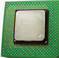
Right, the P4. Well it is green and it has loads of pins. Yep, 423 of them. The
current core which Intel are using, the Willamette, came to market with 1.4 GHz
and 1.5GHz as the native speeds. Then Intel introduced the 1.3GHz unit, and
recently the 1.7 GHz unit. The P4 still has 0.18 Micron cores. It has 42 Million
transistors... don’t believe me? Well count them then ;) The TBird has 37
million and the P3 CuMine has 28 Million.
You all know about the crushed cores we have heard about with AMDs CPUs? Well, I
have hurt 1 myself and I wasn’t happy, but hey, it all happens, I am sure my
friend Kyle at HardOCP can tell you about the fun he hashad with them....
*crunch*. ;)
Intel have put a large heat spreader on top of the unit to help protect the core
and dissipate heat, I am tempted to cut this off to see what is under it... ;)
With this huge Core, and all the new changes, Intel have had a few problems this
unit. The power supplies it uses is a bit funny, I ended up getting an Enermax
to run the beast. It has a new Connector upon the unit... like a Molex cut in 2
and put together. They have also got a different mounting system for the P4 heat
sink, but the CPU didn’t run very hot at all.
The system uses Rambus. We used 2 Rimms of 256MB each, and a thank-you to
Advanced Design for their help sourcing the memory for our test system. We also
had 2 Apacer memory terminators. The memory *has* to go in pairs and it *has* to
be terminated... Got it? RamBUS has large blue heat dissipaters upon the actual
chips.
Enough of the Techno chat lets move on to the testing.
Intel Test Rig :-
Pentium 4 processor at 1.5GHz
ABIT TH7 Raid
2 * 256MB PC800 RDRAM memory modules
Geforce 2 Ultra Graphics card
IBM 60GXP 40GB ATA/100 hard drive
Windows 2000 Professional, Service Pack 1 and DirectX 8.0
AMD Test Rig:-
AMD Thunderbird processor at 1.33GHz
ABIT KT7E Raid
3 * 128MB PC133 memory modules
Geforce 2 Ultra Graphics card
IBM 60GXP 40GB ATA/100 hard drive
Windows 2000 Professional, Service Pack 1 and DirectX 8.0
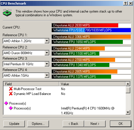
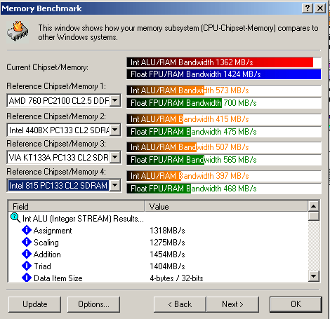
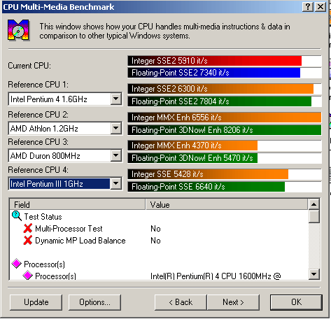
Sandra Results :-
Quake 3 High Quality
| Processor | Score (FPS - higher is better) |
| Pentium 4 (1.5 Ghz Running on 850 Platform) | 120.4 |
| Thunderbird (1.33 GHz Running on KT133A) | 113.2 |
Quake 3 Fastest
| Processor | Score (FPS - higher is better) |
| Pentium 4 (1.5 Ghz Running on 850 Platform) | 238.2 |
| Thunderbird (1.33 GHz Running on KT133A) | 229.2 |
Madonion 3DMark 2000 (1024*768) default.
| Processor | Score (Score - higher is better) |
| Pentium 4 (1.5 Ghz Running on 850 Platform) | 6487 |
| Thunderbird (1.33 GHz Running on KT133A) | 6143 |
(These are just the basic benchmarks as this is what most of you care about ;) None of this Webmark stuff.)
Conclusion.
Yes this unit does have power. Perhaps not as much as the new P4s which will
come out soon, but it is a brand new layout and setup for the system. It does
have its' problems though with the FPU and other features. The Athlon has a far
faster and more powerful FPU unit on it; this is due to the fact of Intel using
SSE2 for the main performance (to avoid using the FPU).
The P4s performance was sure interesting. The memory bandwidth is very
impressive, and its performance in games is good. I had a LAN to go to and the
P4 and an MX kicked out 160 FPS constant with everything on. It was sweet, and
it was hosting an 8 player server at the same time.
Intel are relying on tweaking for the P4 platform to push the sales. This will
happen, but not straight away. The P4 is a beast and it is very powerful, but
the Athlon has the edge at the moment. But don’t hold your breath yet AMD. Both
the platforms would benefit from code optimization.
The current P4 CPUs are a good base performer. It shows that the architecture is
a good idea, but it has to go somewhere. Please also remember that they don’t
have a new FAB for this and it is still made on the same process as the P6
architecture. And it runs at 50% higher clock. The CPU will perform better as
the actual units get faster. Once they hit 2GHz it should be something very
impressive. The technology is good and it does make a good stand against the
Athlon, but it needs tweaking.
The Overclockers in you will probably avoid the P4 unit until Intel shrinks the
die production to the .13 Micron FAB production system. Once they do this there
should be faster P4s on the market which allow more and more people to use the
p4 in powerhouse units. When they shrink the core of the p4 this should also
give a massive performance increase. Once the new P4s are out they will have the
VIA and Intel solutions available which will allow people to run cheaper SDRAM /
DDR Ram memory modules, rather than the expensive RamBUS units. Well, what would
I do... Wait. Get a P4 when they launch the new smaller micron development, or
better still get the 760MP from AMD... dual TBirds should be interesting. Intel
are working on Dual fosters. It would be good to see the performance there. At
Computex this year according to an article here they are going to show the 845
chipset which supports SDRAM on the P4 platform.