We were able to reveal earlier this year that Intel would at last be releasing its answer to general purpose compute modules, such as NVIDIA's Tesla, and that the product would be known as the Xeon Phi and would be built on the firm's 22nm fabrication process.
We were able to elaborate on high-level details, that the system would typically feature above 50 cores, that each core would include a vector unit 512-bits wide and that the system would feature the x86 instruction-set and run Linux. Details that we were seriously lacking were, how exactly did Intel plan on meshing all of this together into a single, functional chip. At the Hot Chips conference, Xeon Phi chief architect, George Chrysos, filled us in.
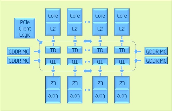
In truth, the bus architecture of the Xeon Phi is not all that dissimilar from IBM's Cell processors. The system features a dual ring-bus, attached to which are GDDR5 memory controllers, a PCIe interface and the compute cores themselves. Where things differ is that, unlike the Cell, where cache was managed in software, compute units in the Xeon Phi feature a large, automated, 512KB Level 2 cache, with a standard TLB implementation. Complimenting these caches are Tag Directories, which allow for independent snooping of all cache on the system. There's a prefetch for large memory transfers, with support for Vector I/O (scatter-graph).
There are other subtle optimisations; each core features an EMU (Extended Map Unit) for accelerating maths functions such as square roots, reciprocals and exponents, somewhat like the special function units found on NVIDIA GPUs. The general idea is that memory controllers will be spaced between the 50 cores to allow for lower-latency and less congested traffic.
If you take 50 cores and assume that each can run at full speed at 2.5GHz, there's potential double-precision number crunching performance of 1 TFLOP - suggesting that unless the final product features more than 50 cores, we'll likely be seeing this clock speed in order for Intel to hit its 1 TFLOP claim.
Of course, how well this device will achieve 100 per cent operating efficiency once unleashed in the real-world is another question altogether. Intel has certainly gone to lengths with its cache implementation, on the other hand, fine-grain control is removed from the programmer and, with a focus on less cores and big vectors, certainly the system isn't optimised for single floating-point calculations, something both NVIDIA and AMD found increasingly common in graphical code.
For many more diagrams and in-depth explanations, take a look at the original presentation document.