


All change, all change
It's been a long, hard struggle, no doubt, but today is a propitious day for AMD. Almost five years after publicly declaring that Fusion - the integration of CPU and GPU on to one piece of silicon - was the only way forward for x86-based chips, AMD now brings it to the masses. The company has settled on APU - Accelerated Processing Unit - for this chip's nom de guerre in the fight against Intel.
Dipping its silicon toe in the waters with the low-power Brazos platform earlier in the year, AMD extends the APU's reach by launching it in mainstream space for notebook computers, with the desktop variant coming a few weeks later. The reason for favouring a mobile launch is simple: it's where the growth is at.
This mainstream APU, which is primed to be the beating heart of laptops priced from $499, has hither been known as Llano. Now productised as the A-Series APU and the main constituent of what is known as the Sabine mobile platform, it pays to take a closer look.
Platform considerations
The aggregation of a CPU and GPU is a clever feat that's also been achieved by Intel with its equivalent Sandy Bridge chips. But neither firms' integration extends to pulling all the necessary inputs and outputs on to one chunk of silicon, and this is why a separate chip, referred to as the Fusion Controller Hub, co-exists with the A-Series APU. Future iterations of the APU will doubtless pull everything together, but for now, both x86 companies use a two-chip mindset.
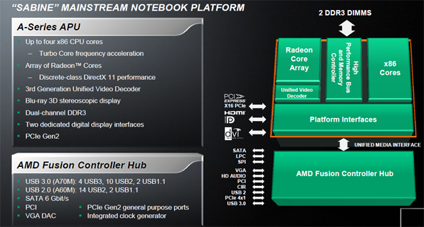
A-Series APU
Stripping it back to basics, the A-Series APU is formed of up-to four x86 CPU cores that are tacked alongside a low-end Radeon-class GPU. This sparse description does AMD's engineers an obvious unkindness, as you will see, but it provides an easy-to-picture idea of what a mid-range APU is all about.
Combined with an array of video and IO outputs along with the handy video-processing block known as UVD 3.0, the APU has practically all the technical jiggery-pokery needed to form an all-purpose processor. The FCH simply adds to the connectivity options that are common fare on modern laptops.
Manufacturing
The overarching purpose of constructing an APU - whether it be for Intel or AMD - is two-fold. First off, bringing the CPU(s) and GPU together should decrease overall cost, once the initial setup costs are set aside. Less silicon is used and, leading on from this, overall power-draw, for a given performance, should drop when compared to a traditional two-chip solution. Secondly, the coupling of the two performance centres should result in greater synergy and, potentially, performance. There's a lot of 'should' in the preceding paragraph, explaining why integration has taken a while.
Lower manufacturing costs and tight coupling are two especially attractive qualities for notebooks manufacturers, who seek to simplify production and release ever-sleeker models. APUs make sense, Intel and AMD agree, but the exact composition of the silicon is where the two companies have divergent views.
While Intel has made remarkable strides in boosting the performance of its anaemic graphics processors, which, as you may know, are now incorporated into the chip with the 32nm-based second-generation Core microarchitecture, the bulk of transistor-count is apportioned for the CPU part.
AMD, however, harnesses the GPU heritage from ATI and opts for roughly a 50/50 transistor split between CPU and graphics cores. This makes sense, too, because the company has a long history of producing feature-rich, low-end Radeon cards that one plugs into the motherboard. Let's lay it all out:
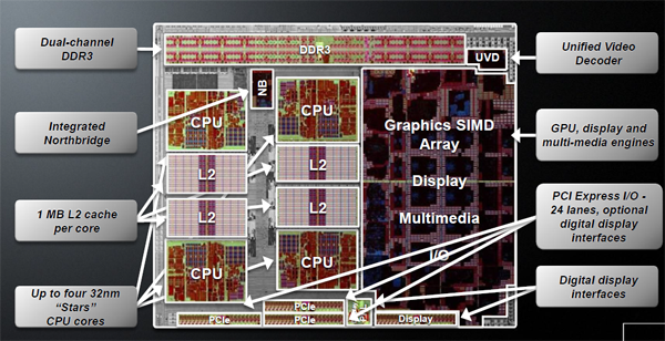
This rather more detailed slide gives clearer insight as to what's happening within the APU. We'll move from the left to the right, wending our way with a greater exposition of the features.
AMD has gone through the complicated, painful process of re-engineering the CPU cores, bringing them together with the GPU - including all the technical juggling that entails - and chosen to do so with a backdrop of moving down a manufacturing process to 32nm, to reduce overall cost.
Marrying the CPU and GPU in concert is fraught with unforeseen danger: there are a goodly number of variables to contend with. The much-needed move to 32nm Silicon-On-Insulator transistor (SOI) technology for the APU has been especially painful, from what we can gather, and we have it on good authority that relations between AMD and manufacturing partner GLOBALFOUNDRIES have been fractious, perhaps underscoring why the A-Series APU is comparatively late in coming to market, much to Intel's glee.
I see STARS
Zooming in to the CPU portion, mobile Llano will ship in two varieties. Straight out of the gate will be a four-core version, as shown above, with a TDP of either 35W or 45W - we'll come to particular models a little later in this discourse - to be followed by a dual-core variant a short while later. The two will be based on different-sized silicon and therefore have distinct die sizes and TDPs. The thinking is that the dual-core Llano chip, complete with a smaller GPU component, will help fill in the performance and TDP gap between the Brazos-orientated APUs and the full-fat Llanos.
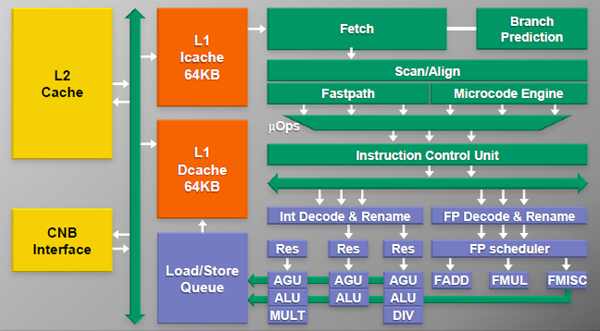
The CPU core architecture is close but not identical to a current Phenom II X4's. AMD needs to fit the cores into a constrained transistor budget, so out goes the fatty L3 cache. This is ameliorated by the doubling of L2 cache, from 512KB per core to 1,024KB. Llano's CPU cores are also tweaked with the inclusion of larger load/store buffers and an improved hardware prefetcher, along with a myriad of other minor improvements.
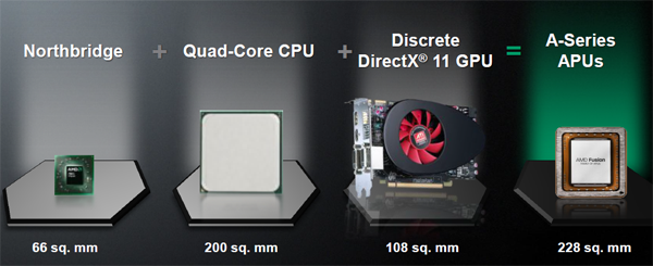
A 32nm process shrinks each core down to a smidge under 10mm², ignoring the associated L2 cache, and the four cores total 140m transistors. Overall, the full-fat Llano chip is 228mm², which, incidentally, is very close to the size of Intel's quad-core mobile Sandy Bridge.
Balancing out the ongoing battle between frequency and power, which is hugely important in a mobile environment, AMD includes Turbo Core support. It enables the cores to run significantly past nominal speeds when there is TDP scope to do so. Granular enough to run on a per-core basis, AMD introduces what's termed a digital APM to control the power states of the APU.
Think of Llano's cores as analogous to a four-core Thuban (well, Zosma) and you won't be too far off the mark.
GPU and UVD 3.0
An APU is nothing without a GPU. AMD's lower-power Brazos platform provided the blueprint by which Llano has been created, and it was inevitable that a fully-fledged Radeon core would find a home on this chip.
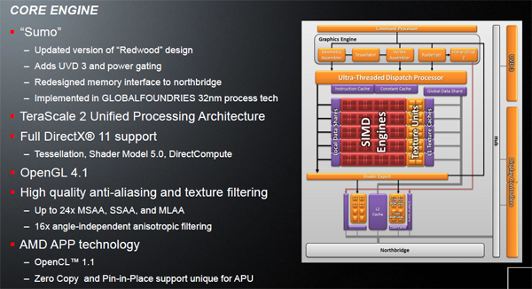
The graphics core in question is remarkably familiar. Based on the Redwood architecture that powers the Radeon HD 5500-series of discrete GPUs, the top-line APU can take in an HD 5570-matching 400 cores. The difference here, if we can call it that, is a shrink down to 32nm, matching the CPUs'. In practically all meaningful ways, then, this is a low-to-mid-range Radeon tacked on to a four-core Phenom II.
You may ask, and we did, why the newer Radeon HD 65xx core wasn't used in this brand-new APU. The reason is rather simple, actually, as AMD needed to finalise the Llano design some time before the release of the latest discrete cards. Providing a bridge between Radeon generations is the UVD video-processing block. Shipping in Llano as version 3.0, therefore matching the 6-series cards, this Radeon is a mix-and-match affair.
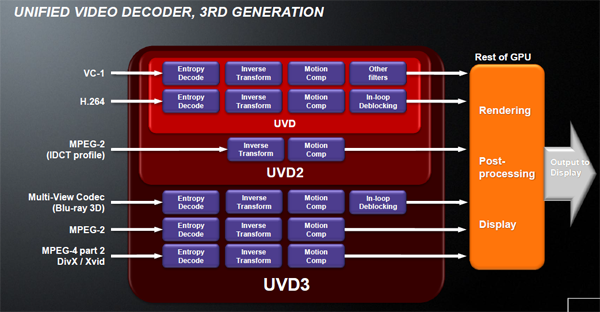
UVD 3.0's new features are shown at the bottom. These include dedicated hardware acceleration for the multi-view codec used for Blu-ray 3D, full MPEG-2 support, and hardware acceleration for DivX and XviD codecs. While these are all decent improvements in their own right, every quad-core CPU is able to handle these in software without significant issue, though the benefits of running them on a super-low-power block will be keenly felt on a mobile chip.
Bringing it all together - the memory-bus architecture
But adding a CPU and GPU on to one die is far more than simply tacking them together. There's the fundamental question of how one apportions the system memory in the least profligate way, for a quad-core CPU and up-to 400-core GPU may both need furious access to it.
One the one hand you have the serial-processing CPU that needs low-latency memory access on an ad hoc basis. On the other there's the GPU, which can hide latencies through execution parallelism but needs lots and lots of bandwidth.
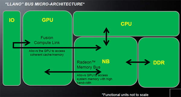
With the CPU running memory requests through the integrated northbridge, AMD's solution is to link both the GPU and CPU to the memory controller. With a dual-channel, 128-bit-wide DDR3 interface sporting memory bandwidth figures of up to 25.6GB/s for mobile (DDR3-1,600) and 29.8GB/s for desktop (DDR3-1,866), the Radeon Memory Bus lets the GPU grab the entire bandwidth, if needed.
And as the GPU and CPU are inextricably bound together, the graphics can access the CPU's memory. The quality of arbitration for system memory is hugely important to the efficiency of the APU. AMD states that the GPU core has 'first refusal' at bandwidth if it's needed, with the CPU getting what's left. This is sensible because the GPU is a colossal consumer of bandwidth, especially when gaming.
Speed, bandwidth and power considerations
Mobile Llano needs to run heck of a lot of processing with a conservative TDP. This is why, on this first mainstream APU, AMD forgoes Turbo Boost support for the graphics; they operate at one fixed speed when under the cosh. However, in the interests of keeping power in check Llano features some nifty power-conserving technology.
First off, while the CPU cores share a single voltage rail, simplifying design, individual cores can be turned off as and when needed (well, to a C6-state). Similarly, there's a shared voltage plane between the GPU, northbridge, UVD block and memory controller, and this plane, and the constituent silicon, can be both frequency- and voltage-reduced. Having individual voltage planes is better and AMD's Turbo Core technology isn't as robust or fine-tuned as Intel's.
Then there's the clock grid itself. Modern chips have multiple frequency zones spread across the silicon. AMD implements what it terms a 'power-aware clock-grid design'. In plain English this means Llano's microarchitecture simplifies zones by removing complex clock buffers and increases efficiency through reducing power-wasting metal capacitance when compared to extant AMD chips.
Display
Any laptop-based all-in-one processor needs to have an eclectic array of display options. Llano has two dedicated display engines - from eight PCIe Gen 2 lanes - that run off the graphics portion of the APU.
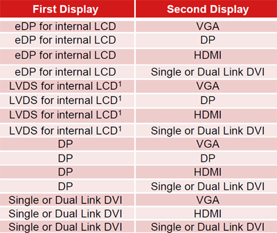
The range of GPU-provided display options is considerable, and it is up to the laptop manufacturer to choose which are plumbed out on their respective models, though they will require a translator chip to use ye olde LVDS. There's also a dedicated x16 PCIe Gen 2 interface from the APU to a discrete graphics card, and an additional four lanes for PCIe expansion connectivity.
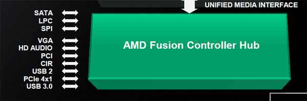
Four further PCIe lanes attach to the Fusion Controller Hub. It has the necessary gubbins to provide SATA 6Gbps, VGA (via a DAC), and, depending upon model, four USB 3.0 ports (A70M). AMD, too, keeps the legacy PCIc ports.
Architecture summary
While plenty of time has been spent of understanding Llano in the preceding paragraphs, it's important not to forget that the APU, in its basic form, is an aggregation of largely existing AMD technologies.
The quad-core CPU, based on Phenom II, has been polished somewhat, while the GPU is taken largely from a Radeon HD 5500-series core. The neat trick here is to pull it all together, manufacture on an advanced 32nm process, and spend significant investment on reducing power-draw and maximising memory-bandwidth throughput on the two competing energy consumers - the GPU and CPU.
Following on the from the above, AMD claims that the APU enables, at worst, Intel-matching battery life in a mid-range laptop, rising up to as much as 10 hours when tuned. We'll be certainly putting this to the test.


