


Bringing it all together
The need for a unified chipset
Intel flexed its technology muscles last week by formally unveiling some nifty next-generation transistor technology, 3D Tri-Gate, which is designed to increase processor performance while reducing power - a rather neat party trick that ensures the chip giant can explore and harvest the benefits of moving down to 22nm and 14nm process nodes. Smaller processes drive transistor density - the building blocks of performance - and this means that Intel's manufacturing prowess is likely to continue for the foreseeable future.
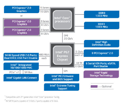
But Intel's still on a 32nm node with the well-received Sandy Bridge processors. Speaking for the consumer, these CPU-and-GPU chips are supported by two main chipsets contained within motherboards, the H67 and P67, collectively known as Cougar Point. While the two share an overriding number of similarities, H67 boards provide display outputs - Flexible Display Interface - by which Sandy Bridge chips' video can be exported to external monitors, while P67 boards, which lack said display outputs, use a discrete video card and tend to have greater voltage and overclocking potential.
Wouldn't it be nice if you could roll the benefits of both the H67 and P67 into one enthusiast-friendly chipset? You'd have all the power and granular control offered by P67 and be able to use the tasty QuickSync video technology provided by H67. And it would be even sweeter if you could properly overclock the CPU, which has shown a propensity to run way past default speeds, when using the IGP.
Z68 is a copy cat
Staggering the chipset launch, Intel is now introducing the Z68, which aims to take the best bits from the present Sandy Bridge-supporting chipsets and then add some unique features of its own. What better way to understand it than to wheel out the venerable, useful block diagram.
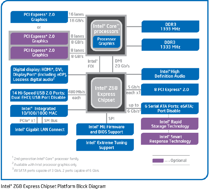
Now, a lot of this will look all-too-familiar to folk who keep up with chipset diagrams. The 'northbridge' - the upper portion of the chipset - is the same as the P67's, mainly because it's all driven from the CPU. This means it uses dual-channel DDR3 memory and can provide up to 16 PCIe lanes for graphics, either apportioned as a single link or bifurcated into two x8 for SLI or CrossFireX. Motherboard partners looking for additional lanes to enable three- or four-way graphics setups will need to add bridging chips.
But Z68's hybrid nature is exemplified by the 'southbridge', which really is an amalgamation of H67 and P67, plus some other goodies on top. The entire left-hand side is a replica of an H67, which means it has support for outputting Sandy Bridge CPUs' video via three digital connections (only two concurrently), made possible by the Flexible Display Interface hook-up to the chip. Swing over to the right and the high-definition audio, eight PCIe lanes, optional RST and six SATA ports - four 3Gb/s and two 6Gb/s - are present on H67 and P67. For those wondering, conventional PCI slots and ATA ports have been long-forgotten.
Look down the bottom and there's a little P67 love in the form of Extreme Tuning Support that enables the user to tweak performance to their heart's content. Pragmatically for Z68, this means you can overclock certain Sandy Bridge CPUs while running integrated graphics; most, if not all, H67 boards precluded such overclocking. What's more, Z68 also allows you to meddle with the clockspeed of the integrated graphics, thus providing frequency and voltage manipulation for the CPU, memory and graphics.
Something really new
The one ace in the pack, Intel hopes, is Smart Response Technology...


