It seems NVIDIA has been having some confidentiality problems over the last month or so, as every other day seems to bring leaked details of a new product. This week it is the turn of the the company's upcoming entry-level chip, the GF108.
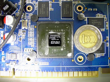
Unfortunately, though, there isn't much to go on beyond a picture. The GPU is clearly marked as a GF108, and appears to be an engineering sample for testing and quality-control purposes. There are four memory chips visible, which could point to a 64-bit memory-bus.
And, further confirming the GPU's entry-level heritage is the fact that the model numbers on the Hynix RAM belong to 2Gb (256MB) DDR3 chips, as opposed to the GDDR5 memory found on other Fermi-based cards.
Of course, there may be another four chips on the other side, doubling the interface up to 128-bit, but that would give the card an unlikely 2GB frame buffer.
Rough guesses on the size of the chip give it an area of around 130mm2. This compares to around 240mm2 for the also unreleased GF106, 367mm2 for the GTX 460's GF104 and a monstrous 529mm2 for the GF100 found in high-end cards. Assuming the chip is built on the same sort of design as the GF104, we would guess that a GPU of that size could support 96 shaders in two 48-shader clusters.
NVIDIA seem to be working pretty hard to bolster its lineup with mid- and low-end offerings based on the Fermi architecture. We're not sure when a card with this GPU will see the light of day, but we fully expect a release date to leak out soon enough.